
2023 Edition
Chapter 20: Thermal
For updates, visit
http://eps.ieee.org/hir
We acknowledge with gratitude the use of material and figures in this Roadmap that are excerpted from original sources.
Figures & tables should be re-used only with the permission of the original source.
The HIR is devised and intended for technology assessment only and is without regard to
any commercial considerations pertaining to individual products or equipment.
March 2023 Thermal
HIR 2023 version (eps.ieee.org/hir) Chapter 20 Page ii Heterogeneous Integration Roadmap
Table of Contents
Chapter 1: Heterogeneous Integration Roadmap: Driving Force and Enabling Technology for Systems of the Future
Chapter 2: High Performance Computing and Data Centers
Chapter 3: Heterogeneous Integration for the Internet of Things (IoT)
Chapter 4: Medical, Health and Wearables
Chapter 5: Automotive
Chapter 6: Aerospace and Defense
Chapter 7: Mobile
Chapter 8: Single Chip and Multi Chip Integration
Chapter 9: Integrated Photonics
Chapter 10: Integrated Power Electronics
Chapter 11: MEMS and Sensor Integration
Chapter 12: 5G, RF and Analog Mixed Signal
Chapter 13: Co-Design
Chapter 14: Modeling and Simulation
Chapter 15: Materials and Emerging Research Materials
Chapter 16: Emerging Research Devices
Chapter 17: Test Technology
Chapter 18: Supply Chain
Chapter 19: Cyber Security
Chapter 20: Thermal
1.0 Introduction and Scope .................................................................................................................................. 1
2.0 Canonical Problems with Thermal Challenges .............................................................................................. 1
3.0 Advanced Technologies and Research Innovations ..................................................................................... 17
5.0 References
................................................
....................................................................................................
34
Chapter 21: SiP and Module
Chapter 22: Interconnects for 2D and 3D Architectures
Chapter 23: Wafer-Level Packaging, Fan-in and Fan-out
Chapter 24: Reliability

March 2023 Thermal
HIR 2023 version (eps.ieee.org/hir) Chapter 20, Page 1 Heterogeneous Integration Roadmap
Chapter 20: Thermal
1.0 Introduction and Scope
Heterogeneous Integration poses several significant challenges for
thermal management at multiple length scales ranging from heat
extraction from hot spots, heat transfer through multiple layers of
materials, different target temperatures for specific devices/materials,
to heat rejection to a system cooling solution or the ambient. This
Technical Working Group (TWG) considers three areas for thermal management:
• Die level;
• Package integration/System-in-Package (SIP)/module level;
• System level (limited to board and server level).
In addition to the taxonomy of the physical categories listed above, this chapter will focus on articulating the
following in quantitative (wherever possible) and qualitative terms:
Canonical problems with thermal challenges;
Cooling limits for known solutions;
Advanced concepts and research.
2.0 Canonical Problems with Thermal Challenges
In the 2021 chapter, we included several canonical problems with thermal challenges, including the thermal
challenges within 2D and 3D stacked dies, optics/photonics-based heterogeneous packages, voltage regulators in a
heterogeneous package, as well as the applications within harsh environment and mobile chipsets.
In this 2023 chapter, along with the canonical problems, we will focus on the following new updates:
Emerging challenges and opportunities for thermal modeling for advanced 3D IC systems;
Challenges and characterization of hotspot modeling;
Thermal modeling on High Bandwidth Memory (HBM) stacks;
Thermal challenges related to integrated voltage regulators (IVRs);
Innovative methods for manufacturing silicon microchannels.
c
Prior to discussing the canonical problems in detail per the discussion from the 2021 version of this chapter, and
to provide an illustration of the dramatic future thermal challenges in the area of thermals, nominal Thermal Demand
Envelopes are displayed in Figure 1 [1], which indicate that thermal technologies must cover a Hotspot Density
Envelope in the 2x-4x range (higher than the supported average power density), with an understanding of the impact
of hotspot area relative to total die area, overall thermal design power and upside capability for both 2D and 3D
architectures.
Figure 1: Nominal Thermal Demand Envelopes covering average and hotspot peak power density
for both 2D and 3D Architectures [1 W/mm
2
= 100 W/cm
2
]
Send corrections, comments and
suggested updates to the TWG chair,
using our HIR SmartSheet:
https://rebrand.ly/HIR-feedback

March 2023 Thermal
HIR 2023 version (eps.ieee.org/hir) Chapter 20, Page 2 Heterogeneous Integration Roadmap
It is important for the thermal community to identify and develop a detailed understanding of the capabilities and
limitations of key thermal technologies that meet or exceed these demands so that they are available well in advance
of need and can be implemented if they meet integration cost envelopes.
2.1 Thermal challenges in 2D packages
Figure 2 shows the 2D enhanced architecture (2D-EA) as a part of the overall 2D-3D packaging taxonomy.
2D-EA can be divided between 2D Organic (2DO) and 2D Passive Silicon (2DS).
The 2DO architecture can be further divided to Chip Last and Chip First. Chip Last is also known as RDL
(redistribution layer) first and is a process where the device wafer is bumped and then diced, and flip-chipped to RDL
that is formed on a temporary carrier. Chip First is a process where dice are reconstructed on a wafer, embedded in
mold compound and followed by the RDL forming process. For detailed discussion, see Chapter 23 on WLP.
The 2DS architecture can further be divided between without and with through-silicon vias (TSVs).
Figure 2: 2D-3D packaging taxonomy [2].
2D-EA is a side-by-side heterogeneous integration of two or more functional components (ASIC, FPGA, CPU,
GPU, single or 3D-stacked memory) using an organic or inorganic interposer or an embedded high-density
interconnect-enabling connector (e.g. Embedded Multi-die Interconnect Bridge, EMIB), as shown in Figure 3.
Figure 3: Schematic of 2D-EA [2].
March 2023 Thermal
HIR 2023 version (eps.ieee.org/hir) Chapter 20, Page 3 Heterogeneous Integration Roadmap
In summary, these are the thermal challenges for the 2D heterogeneous-integrated packages:
Increasing package power density;
Increasing total package power dissipation;
Thermal cross-talk, including the need for thermal isolation;
Different thermal (Tj) requirements and sensitivities;
Thermal interface material (TIM1 or TIM1.5) thermal insulance (K-mm
2
/W) uncertainty from increasing
form factor and Si surface flatness and overall warpage impact;
Enabling good thermo-mechanical performance;
Interposer thermal properties (glass/Si/organic) (see Figure 3) including anisotropy;
Interposer thermal conductivity has a strong impact on the chip thermal resistance;
Glass and Si interposer performance can be made comparable, by appropriate enhancements;
Interposer heat spreading and heat removal.
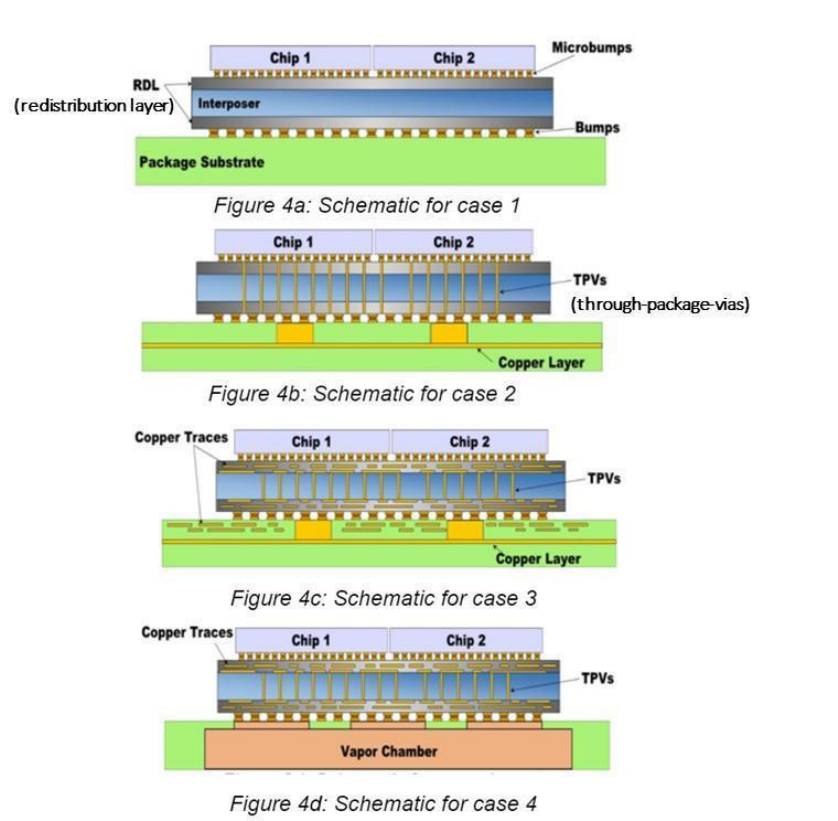
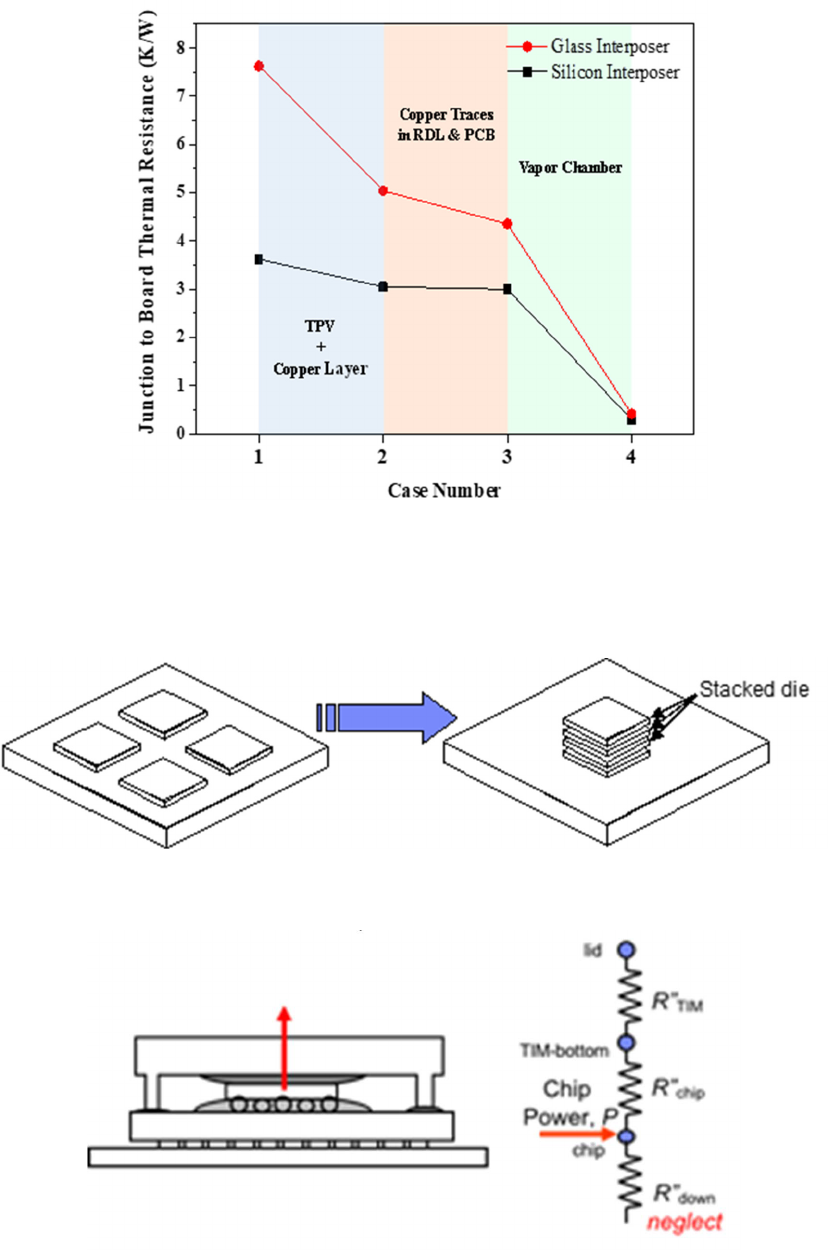
Figure 4 depicts several different cases that are analyzed, with the thermal results mapped in Figure 5.
Figure 4: Multiple 2D configurations for thermal assessment [2].
Figure 5 displays the results from analyzing cases 4a - 4d depicted in Figure 4 and illustrates that with internal
thermal enhancements, and coupling with effective heat removal pathways, glass interposer performance could be
made comparable to silicon interposers. Glass interposers have other attractive features including better high
frequency signaling characteristics, and lower manufacturing costs due to panel fabrication. So this thermal
enhancement may make glass a more attractive technology for the reduction in junction-to-case thermal resistance
(K/W).
March 2023 Thermal
HIR 2023 version (eps.ieee.org/hir) Chapter 20, Page 4 Heterogeneous Integration Roadmap
Figure 5: Impact of interposer and substrate thermal conductivity on package thermal resistance [3].
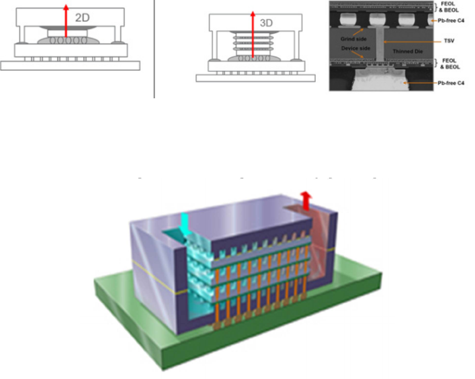
2.2 3D stacked-chip packages with conduction interfaces
Thermal management is critical in the design of high-power 3D stacked-chip packages which enable high-
bandwidth and low-latency communications. By stacking chips, as shown in Figure 6, the effective power density
increases because the power generated in the 3D stack has to be dissipated over the “footprint” area of a single chip.
Figure 6. Effective power density increases in a 3D stacked package
In a high-power 2D package, shown in Figure 7, most of the heat generated in the chip conducts through a thermal
interface material into a metal lid and then externally to a heat sink.
Figure 7. Conduction paths in a high-power 2D package
In a high-power 3D package, heat from the bottom chips in the 3D stack has to conduct through additional
materials that form the interconnect/underfill layers, the back-end-of-the-line (BEOL) layers, and the bulk silicon
above the BEOL layers. This causes additional thermal resistances in the heat conduction path as depicted in Figure
8.

March 2023 Thermal
HIR 2023 version (eps.ieee.org/hir) Chapter 20, Page 5 Heterogeneous Integration Roadmap
Figure 8. Conduction paths in a high-power 3D package
Additional increase in temperature in a 3D chip package can occur due to vertical alignment of high-density
computing cores and different-sized stacked chips. Alternatively, such a chip stack can be cooled from both top and
bottom, offering a 2x improvement in cooling capacity but at the cost of a far more complex design.
A highly relevant example of a 3D stacked die package that is prevalent in the industry is the High Bandwidth
Memory (HBM) that is depicted in Figure 9 [4]. Figure 9 illustrates a sample System-in-Package that comprises a
CPU or GPU Processor and a stacked die HBM, on a shared silicon interposer, with the sub-assembly residing on a
PCB. As may be surmised from the preceding discussion of Figure 8, the stacked-die HBM poses significant cooling
challenges for the removal of the heat dissipated through conduction in the vicinity of the heat sources. As is also
evident from Figure 9, the efficacy of heat removal from such stacked dies can enable increased memory capacity
through greater stacking of memory dies (2- to 4- to 8-high stacks).
Figure 9. Example of a Heterogeneously Integrated Package with 3D stacked die High Bandwidth Memory.
Examples of 2, 4, and 8 High Stacked Die HBMs [4]
2.3 3D stacked die with embedded liquid cooling
To continue scaling computer performance as Moore’s Law transistor scaling slows, the IT industry has turned to
3D chip stack interconnect technology, which both increases the bandwidth between chips and enables heterogeneous
integration to improve computing performance. However, the stacking of chips presents new thermal challenges as
heat generated by multiple chips within a chip stack results in higher heat density which must be effectively removed.
The traditional approach of 2D chip thermal management is to conduct the heat from the active devices through
the silicon die to a heatsink or cold plate which is attached to the top (or backside) of the chip with a thermal interface
material as shown in Figure 10(a). The conduction of heat through a 3D chip stack as shown in Figure 10(b) creates
March 2023 Thermal
HIR 2023 version (eps.ieee.org/hir) Chapter 20, Page 6 Heterogeneous Integration Roadmap
a thermal challenge, since the heat must conduct through multiple dies within the stack. Heat generated by the Nth
die in a chip stack will conduct heat through N-1 dies to reach the heatsink or cold plate placed upon the top of the
first die in the chip stack. It is important to note that the dies include complex structures including the Front-End-of-
the Line (FEOL), Back-End-of the-Line (BEOL) with multiple wiring levels, and Through-Silicon-Vias with µC4
interconnects between them, as also shown in Figure 10b. These structures, when stacked and assembled with the
usual placement and alignment tolerances, dramatically increase the thermal resistance between the dies in the stack
and the heatsink or cold plate placed on the top die in the stack.
Figure 10: 2D vs 3D Thermal Path
While conducting heat through a chip stack can provide effective thermal management for stacks of low-power
chips, when stacks include one or more high-power chips within the stack the conduction of heat through the dies
and interconnects in the stack can produce high gradients in the chip junction temperatures across the stack. A method
to address the challenges of cooling 3D chip stack structures described in this section is embedded cooling, where
coolant flows either within (intrachip) or between (interchip) the stacked high-power chips as shown in Figure 11.
Figure 11 Embedded cooling with liquid flow internal to a 3D stacked chip package
Embedded cooling creates new requirements for 3D chip stack co-design, including placement and dimensions of
fluidic channels, coolant properties, and compatibility with chip stack power and signal electrical interconnects. The
fluid channel heights may be guided by compatibility of fabrication processes to create electrical interconnects
between dies in the stack layers. For example, parallel channels with dimensions which meet the electrical
requirements can create substantial pressure drop when using a single-phase liquid to flow across 20 mm (or more)
for large processor dies. Use of the most conventional liquid coolant, water (which is conductive), requires the need
to isolate the fluid from power and signal electrical interconnects and also consider dielectric losses associated with
transmitting high frequency signals nearby. These challenges are part of the electrical, mechanical and thermal co-
design of embedded cooling in a 3D chip stack.
2.4 Thermal challenges in photonic devices
Photonic devices as shown in Figure 12 can have high power density and require novel approaches to thermal
solutions. Thermal challenges associated with photonic devices pertain to both the temperature swing and the
absolute operating temperature of a given device. Depending on the component and use conditions, either one or
both criteria may limit its performance. For example, optical modulators often depend on interference and resonant
effects. Resonant modulators, which are useful to reduce the energy per bit, are mainly limited by the temperature

March 2023 Thermal
HIR 2023 version (eps.ieee.org/hir) Chapter 20, Page 7 Heterogeneous Integration Roadmap
swing (typically < 30°C), whereas oscillators such as laser sources are limited by both the temperature swing
(typically < 30°C) and the absolute operating temperature (typically < 100°C) [5]. In addition, photonic devices can
be integrated with other functional IC components at the chip and/or package/system level. These components may
have different thermal specifications which require both package and system thermal solution optimization.
Figure 12: Heterogenous packaged photonics with stringent temperature control challenges [6]
2.5 Heterogeneous Integration for Harsh Environments
2.5.1. Aerospace, automotive and space harsh environment requirements
As the world is getting more digital – through such trends as IoT, autonomous vehicles, AI and electric drive –
safe and reliable operation of electronics in harsh environments such as aerospace, automotive, and space are
becoming more and more critical.
In order to let compute systems take control of assets that can impact the safety of persons and/or cost millions of
dollars, strict standards of hardware and software system safety must be taken into account. Harsh environment
electronic applications must typically satisfy stringent requirements to operate safety-critical applications in extreme
temperature, dust, vibration, and corrosive environments for operational periods of 10 to 30 years. In an example of
harsh environment electronics, aerospace class I electronics need to operate in a continuous ambient environment of
-54°C to 55°C and survive a temporary 30-minute ambient environment of 71°C, without cooling air supply,
simulating a cooling air supply fault condition.
In the automotive environment, burn-in and test of heterogeneous or multichip systems is a particular challenge.
Test temperatures are extreme because of the harsh environments that these systems must operate in, sometimes
ranging from -55°C to 175°C. For automotive power electronics, the research focus and target is to increase the
power density to 100 kW/L and double the reliability from 150,000 to 300,000 miles, while lowering the cost of
power electronics, electric motors and the overall traction drive system by 2025 [7]. This power electronics power
density increase to 100 kW/L represents a factor of 5 to 10 increase with respect to the state-of-the-art electric-drive
vehicle power electronics.
Satellites are increasingly using power-hungry devices such as earth observation detectors operating in new or
multiple frequency bands. The higher frequency bands currently under consideration for next-generation
transmission systems offer higher bandwidths than the longer-wavelength bands currently in use. At the same time,
those shorter-wavelength bands by nature have larger propagation losses. Challenges in space requirements involve
the impact of solar heating and space radiation with the potential of significant thermal cycling of the electronics
package, which is especially challenging for heterogeneously integrated packages.
Application of heterogeneous integration to harsh environments is challenging due to the 3D top-side contour of
heterogeneous packages, the dissimilar junction limits of heterogeneous components in a system, and the extreme
thermomechanical challenges imposed by the extreme temperature cycles. However, due to superior performance, it
is likely only a matter of time before these challenges are overcome and heterogeneously integrated chips make their
way into the harsh environment of space.
2.5.2 Heterogeneous integration top side cooling solution needs
Rugged harsh-environment electronics rely predominantly on heat rejection through a thermal interface layer and
a heat spreader mounted over the flip-chip package. This thermal interface layer serves to thermally connect
components of dissimilar coefficient of thermal expansion (CTE) such as silicon (chip) and aluminum or copper (heat
spreader). As ruggedized electronics typically are produced in moderate volumes (100s-1000s), chip height, chip
warpage and other non-planarity variations batch to batch of several hundreds of microns can be typical due to ball

March 2023 Thermal
HIR 2023 version (eps.ieee.org/hir) Chapter 20, Page 8 Heterogeneous Integration Roadmap
grid array (BGA) and silicon variations. The thermal interface material also serves to compliantly compensate for
these differences by filling gaps and ensuring good thermal contact between these components.
As heterogeneous integration introduces 3D non-planar and large silicon structures, challenges can be envisioned
in connecting to a top-side heat sink using current thermal interface materials. It can also be expected that as multiple
micro-BGA connections are used to create vertical stacks, height and planarity variations will accumulate, resulting
in amplified variance in the eventual location of the top-side chip interface as illustrated in Figure 13.
Figure 13: Notional 3D chip architecture and anticipated topology challenges
To manage this, novel 3D thermal interface, material systems are envisioned. De Bock et al. [8] describes such a
thermal interface system that uses a thicker layer of low melting point (LMP) solder, encapsulated by an ultra-thin
micro layer of a high-temperature polymer. When pressure is applied during heating, the LMP solder flows and
conforms to the chip shape while being contained by the thin polymer “bag” as illustrated in Figure 14. When the
containment layer polymer is sufficiently thin, its detrimental contribution to the TIM thermal resistance can be
sufficiently small, outweighed by the superior thermal conductivity of LMP solders like Indium (k ~ 70 W/m-K),
which exceeds common thermal interface materials.
Figure 14 Encapsulated LMP solder thermal interface system with the potential to conform to 3D chip topology
As LMP solder never comes in full contact with the silicon chip, no intermetallics are formed, eliminating the
need for barrier coatings and allowing for re-workability. The benefits of such a concept are the ability to compensate
for chip height and angle variation, non-planar chip warpage, and 3D topologies.
2.5.3. Dissimilar heterogenous component systems solutions
In automotive power conversion, a target of power density increase to 100 kW/L is envisioned to be achievable
by downsizing the components and managing device heat fluxes on the order of 1000 W/cm
2
. In addition, increasing
the temperature of the wide-bandgap (WBG) devices up to 250°C is an important enabler towards meeting the goals
of downsizing the components. This is a heterogeneous integration thermal management challenge since multiple
components with different functionalities and temperature limits (transistors, diodes, capacitors, gate drivers, other
passives) need to be packaged within a small volume. Hybrid silicon and WBG technologies and configurations are
also of interest – and this is another heterogeneous integration challenge or problem.
Figure 15 shows a schematic of an inverter in which the different components are in a stacked, multilayered,
compact configuration. A power module or package incorporating WBG devices is desired that can operate at device
junction temperatures up to 250°C. This will require significant advances in WBG device technology, circuit boards,
advanced interface materials and interfaces (likely bonded interfaces), electrical interconnects, encapsulants,
electrically-isolating substrates, as well as novel baseplate and heat exchanger materials that can withstand the higher
temperatures, give good thermal performance and also have mechanical properties that ensure good reliability for the
system (the target numbers have been listed above).

March 2023 Thermal
HIR 2023 version (eps.ieee.org/hir) Chapter 20, Page 9 Heterogeneous Integration Roadmap
Figure 15: Inverter in a multi-layered board or stack-up configuration
Some components such as gate drivers and capacitors have lower temperature limits – as the state of the art stands
in terms of materials capabilities – of approximately 125°C or lower. In order to package these passive components
– utilizing in-board, stacked 2- or 3-D packaging concepts – in close vicinity of the higher-temperature (e.g. 250°C)
semiconductor device or package, advanced thermal management techniques will be required. These include fluid-
based cooling technologies, and also concepts such as manipulation of heat flux lines (e.g. metamaterials) so as to
divert or block the heat flow to lower-temperature-rated components. There is scope for innovation in the fluid-based
cooling technologies; two-phase cooling through passive/pool boiling or forced convective boiling, vapor chambers,
heat pipes, and perhaps even fluid-cooling utilizing dielectric fluids within the transistor and diode need to be
investigated.
Thermal management of electrical interconnects is an important way to keep the capacitor temperatures within
limits [9]. Heat typically flows to the capacitors from the packages/devices/power modules via the electrical
interconnects (Figure 15) and thermally managing the interconnects is important for inverter/converter system-level
thermal management as well.
Higher voltages are also being considered as a means to downsize the footprint and increase the power density of
the power electronics. This will require development of appropriate electrical isolation for the higher voltage, which
could have thermal management implications as well. Either the material or the thickness/footprint of the electrical
isolation will have to change, and thermal solutions will have to be developed or adjusted accordingly to ensure good
thermal performance and reliability as well as to maintain a compact footprint.
2.5.4. Heterogeneous integration thermo-mechanical solutions
Satellite phased-array antenna-in-package solutions offer increased efficiency for higher power applications;
however, heat dissipation remains a challenge. Materials in the signal propagation path must be dielectric to minimize
signal losses, limiting the applicability of topside cooling strategies. Penetrations in the PCB, and heat sinks with
pedestals, have been proposed to bring cooling to the package for these high-power applications [10]. However, in
the vacuum environment of space where convective cooling is not available, the need for compliant interface
materials that can make contact with an array of discrete components while not suffering performance losses due to
the lack of convective enhancement remains a critical need.
In addition to AiP challenges in the space environment, satellites in low earth orbit (LEO) may deploy onboard
FPGA system-in-package solutions to enable services such as on-board signal or image processing and 5G internet.
Because their orbit is not geosynchronous, these devices typically operate intermittently and dissipate a large amount
of heat locally for a short amount of time. Sizing a radiator of the small-LEO satellites for peak heat loads results in
excessive area requirements and results in components becoming too cold in non-operating conditions. Furthermore,
these components are generally located in the interior of the satellite, without direct access to a radiator. Over time,
thermal fatigue also becomes a significant challenge, especially with CTE-mismatched heterogeneous structures.
When coupling high-power components to the radiator via heat pipes is not an option, local thermal storage using
phase-change materials or other high specific-heat-capacity solutions that minimize required system launch weight
may become attractive solutions.
At the same time, traditional interfacing strategies for test, including the use of liquid thermal interfaces or dry
interfaces, are no longer viable because the varying die heights would result in components with no contact to the
thermal control unit (TCU). To fill the gaps between the multiple die and the TCU, durable, compliant, low-
compression-set interfaces are required. Silicone-based materials offer the mechanical properties that these
applications demand (wide operating temperature range, forgiving compressive mechanics); however, the risk of
silicone contamination of the device under test drives the need for new solutions. Aligned, conductive nanosprings,
such as carbon nanotube arrays impregnated with polymers, may offer a path forward [11], if they can offer the long-
range compressibility (for package die
height v
ariations on the order of 100s of microns) as well as low compression

March 2023 Thermal
HIR 2023 version (eps.ieee.org/hir) Chapter 20, Page 10 Heterogeneous Integration Roadmap
set (to address variation in package-to-package height driven by manufacturing tolerances) that these emerging
technologies demand.
2.5.5 Heterogeneous integration in harsh environments: conclusion
As with most electronics lifecycles, operation of new technology often starts in highly competitive applications
with limited operational life, of which some can be consumer electronics. As these technologies mature and gain
more pedigree, more and more application to critical electronics in harsh environments can be considered. This study
identified three areas of technology research that can be focused on to further aide this progression. These are the
development of 3D thermal interface technology, application of CTE-matched heat spreaders, and active transient
thermal hot spot management. It is anticipated that with time and development support, these technologies will
further advance, allowing one day for safe and reliable operation of heterogeneously integrated electronics in the
transportation, industrial and other safety-critical systems of tomorrow.
2.6 Thermal challenges in mobile platforms
The shrinking form factor of mobile electronic devices in conjunction with significantly increasing performance
and functionality have resulted in substantial thermal challenges. Nelson and Galloway [12] report reduction in
thickness of Smart Phones from about 25 mm to less than 10 mm while power has increased from below 3 W to about
7 W for the latest devices. The total number of packages inside such smartphones have also grown over several
product generations to about 70 [12]. Figure 16 [12] shows the external surface temperature profile for a commercial
smartphone and illustrates the presence of a significant hotspot at the location of the processor.
Figure 16: Temperature contour data for the external surface of a smartphone [12]
Steady state and transient thermal characteristics and spreading from hot spots primarily through conduction
(copper, PCB, silicon, TIM) are reported to be key drivers for thermal design [12] with dynamic thermally-aware
power throttling being an effective control technique for thermal management. Figure 17 provides an inside view of
a State-of-the-Art Smart Phone [12] and shows a micro heat pipe spreader attached to multiple devices and packages
to promote heat spreading from multiple heat sources. Graphite sheets and copper “straps” have also been harnessed
to this task.
Figure 17: Micro heat pipe in a modern smartphone [10]
2.7 Thermal challenges in voltage regulators
Scaling trends and device refinements indicate gradual and steady transition to lower-threshold voltage regulator
devices, driving up package-level current to several 100s of amps. Ohmic losses on power delivery connections tend
to dominate the power dissipation. However, local decoupling needs exacerbate the challenges associated with higher
voltage DC distribution and down-conversion to required DC levels with regulators on/near die (and on-die) within
the package. Thus, one of the power devices that can be part of a heterogeneously integrated package is a VR (Voltage
Regulator) such as what is depicted in Figure 18. Such power devices inside the package are potential hot spots and
March 2023 Thermal
HIR 2023 version (eps.ieee.org/hir) Chapter 20, Page 11 Heterogeneous Integration Roadmap
create a significant cooling imperative. For example, even at 95% efficiency, a 200W VR will dissipate 10 Watts,
mostly within the power switching devices with a small footprint inside the package.
Figure 18: Package level DC to DC VR schematic
2.8 Emerging challenges and opportunities on thermal modeling and simulation for advanced 3DIC system
With the recently introduced wafer level front-end 3DIC chip stacking technology, such as TSMC’s SoIC (System
on Integrated Chips), in Chip-on-Wafer (CoW) or Wafer-on-Wafer (WoW) stackings can now be assembled with
backend 3DIC technologies such as Chip on Wafer on Substrate (CoWoS) or Integrated Fan-out (InFO), as shown in
Fig. 19 [13]. Other foundries offer similar technology roadmaps [14].
Figure 19: Industry trend of integrated frontend + backend holistic 3D heterogeneous integration
Several emerging design optimization techniques for thermal consideration are needed for the new generation of
3DICs with closely packed chiplets and strong cross-die thermal coupling. The most important is the use of Dynamic
Thermal Management (DTM) with thermal throttling via DVFS (Dynamic Voltage Frequency Scaling) techniques.
Advanced 7nm/5nm designs normally have many on-chip thermal sensors to monitor the chip temperature behavior;
for example, the Vega 2.0 3DIC from AMD has 64 on-chip thermal sensors in-place, as shown in Fig. 20. This
implies that an accurate static and transient thermal simulation is needed with a fine mesh grid to optimize the
placement of on-chip thermal sensors.

March 2023 Thermal
HIR 2023 version (eps.ieee.org/hir) Chapter 20, Page 12 Heterogeneous Integration Roadmap
Figure 20 Many more on-chip thermal sensors are placed in advanced CPU/GPU 3DIC such as the Vega2.0
from AMD for DTM through fine-grain DVFS control.
Another emerging need of advanced 3DICs is the early estimation of static and transient thermal hotspots with
transient-based partitions of power in discrete chips in a 3DIC. The thermal interaction is particularly significant in
vertically stacked dies as in SoICs with Chip-on-Wafer or Wafer-on-Wafer stack-up. Therefore, an architecture-level
static and transient thermal simulation is required with the transient power profile of different chips computed from
the vectors generated from emulation, as shown in Fig. 21. Co-optimization of testing sequence and thermal/Vdroop
during shift-in and at-speed testing is another emerging challenge for advanced 3DICs as shown in Fig. 22.
Figure 21: Architecture-level fast static and transient thermal simulation is required to help optimize the
transient power partition of chips in 3DICs during boot-up sequence or peak functional vector operation

March 2023 Thermal
HIR 2023 version (eps.ieee.org/hir) Chapter 20, Page 13 Heterogeneous Integration Roadmap
Figure 22: Testing of large 3DIC consisting of CPU/GPUs, etc. presents a major challenge due to multiple localized
thermal hotspots and dynamic voltage drop. Co-optimization of test techniques and thermal/Vdroop is required.
It is well understood that thermal issues can severely degrade the performance and reliability of a chip and thermal
runaway may occur if the temperature-dependent leakage power increases exponentially with increasing localized
temperature at certain areas in a 3DIC. A large value of peak temperature and thermal gradient on-chip caused by
localized hotspot and cross-die thermal coupling can have a severely negative impact on transistor performance,
stress, aging, electromigration (EM), voltage drops, and timing. Therefore, the following are the challenges and
opportunities on thermal modeling and simulation for advanced 3DIC systems:
Performing fine-grained static and transient thermal analysis on large 3DIC designs is required and demands
adaptive meshing or machine-learning technology to overcome the limitation using traditional CFD/FEA
based solvers [15][16][17][18].
Architecture-level thermal and thermal-induced stress analysis are required due to the thermal coupling from
cross-die horizontally and vertically with transient-based power profile among chiplets in 3DIC. Thermal-
induced stress and warpage can impact the performance of circuits such as in C4 bumps, microbumps,
TSVs, extreme low-K dielectric, etc. particularly for large 3DICs.
Heterogeneous Integration 3DICs may consist of analog/mixed-signal and digital designs which have very
different thermal and stress requirements that need to be co-optimized among chiplets and package in
3DICs.
For Silicon Photonics 3DICs, accurate thermal gradient analysis is required for the co-optimization of 3DIC
package and required thermal heater for PIC design.
Testing of large 3DICs consisting of CPU/GPUs, etc. presents a major challenge due to multiple localized
thermal hotspots and dynamic voltage drop affecting yield. Co-optimization of test techniques and localized
thermal hotspots and Vdroop on 3DICs should be considered.
2.9 Modeling on-chip hotspots: Challenges and characterization methods
On-chip thermal hotspots are a growing concern for modern heterogeneous computing systems, especially systems
with stacked dies and advanced packaging. It is well known that, as process technology scales, increasing power
density has been stressing the power and cooling limits of modern microprocessors. Advanced hotspots not only
have high absolute temperatures, but they are also fast, localized, highly non-uniform, and application dependent.
Figure 23 shows the distribution of the amount by which per-pixel die temperature changes over 200 μs intervals for
14nm compared to 7nm [19]. The 7nm die is worse in two ways. First, the peak change in temperature is greater,
resulting in faster temperature spikes. Second, the variance in temperature deltas is wider, indicating the potential
for large temperature deltas. All of these changes take place over only 200 μs, indicating that techniques to mitigate
hotspots will need to be even more aggressive than they previously were, resulting in the need for increased guard-
bands at the cost of dramatically decreased performance.

March 2023 Thermal
HIR 2023 version (eps.ieee.org/hir) Chapter 20, Page 14 Heterogeneous Integration Roadmap
Figure 23a: Distributions of changes in on-chip temperature every 200 us.
Hotspots need to be studied in a fast end-to-end manner. New integration methods (e.g. 3D stacking, interposers
and chiplets) have cooling challenges that could exacerbate hotspots. New memory technologies and mixed-signal
circuits are more sensitive to temperature fluctuations. Over the next few years the industry will need to (1) build
fast thermal models; (2) improve formal methods to characterize hotspots between applications and systems; and (3)
develop new methods to predict and manage hotspots.
While the research community has several open source power models [20] and thermal simulation models [21,
22], integrated and combined validated flows with clear interfaces are needed because of the coupled nature of thermal
and power. The HotGauge hotspot characterization framework is one of the first such open source integrated efforts,
shown in Figure 23b [19]. HotGauge integrates power, performance and thermal models with novel hotspot
characterization methods. These characterization methods measure not only the magnitude of the hotspot but its
gradient. Initial case studies with HotGauge simulated an Intel Skylake-style processor in 14nm, 10nm, and 7nm and
demonstrated hotspot behavior and severity across applications.
Figure 23b: Characterizations of thermal hotspots require integrated performance, power and thermal simulation tools
combined with standardized characterization methods. This figure describes an example tool, HotGauge.
In-order to compare designs and implementations, the research community needs new formal hotspot definition
and characterization methods. Current hotspot characterization methods focus on the magnitude of the hottest point
and not the size of the thermal gradient that indicates the speed of the hotspot and its propensity to cause timing
failures or reliability issues. HotGauge introduces a formal definition that uses the temperature of the hotspot with a
new maximum localized temperature differential (MLTD) that captures the maximum gradient with a defined radius
(either a core or 1mm distance). HotGauge defines a hotspot severity metric, Figure 24, which combines the MLTD
of the hotspot with its magnitude, with three configurable sigmoid functions that could be used in a predictor or a
control system. The severity metric captures intuitively how extreme hot spots on the chip (e.g. > 100°C) are
concerning and points of moderate temperature (e.g., 80°C) with high gradients (MLTD > 25°C) are also concerning
because of timing failures and the speed of the hotspot.

March 2023 Thermal
HIR 2023 version (eps.ieee.org/hir) Chapter 20, Page 15 Heterogeneous Integration Roadmap
Figure 24: Hotspot severity which combines the max temperature and worse MLTD
2.10 Thermal modeling for high bandwidth memory (HBM)
High Bandwidth Memory (HBM) consists of a buffer die and core die (memory), and the stacked dies are
connected with through-silicon vias (TSVs) as shown in Figure 25. HBM has been widely used in high performance
computing; however, HBMs are generally challenging to cool due to the large stack thermal resistance and thermal
coupling (or thermal crosstalk) from high power logic chips close by, which might have higher operating temperature
limits than that of HBMs. On the other hand, due to HBM’s complicated stacking structure, HBM is also not easy to
simulate and obtain accurate temperature predictions.
Figure 25: Stacked structure of HBM
Figure 26 shows a simplified thermal modeling method, which potentially can accurately predict the HBM thermal
resistance and temperature with limited computational effort.
Figure 26: Thermal conductivity extraction process 3D heat flow considered
The method extracts the effective thermal k for each HBM layer by building a cookie model including all the
BEOL and joint details, and using the effective thermal k for the integrated HBM thermal model. The method has

March 2023 Thermal
HIR 2023 version (eps.ieee.org/hir) Chapter 20, Page 16 Heterogeneous Integration Roadmap
been validated with testing results and has shown that the accuracy can be around 97% compared to the detailed
model [23].
Figure 27 shows a case study to quantify the impact of HBM temperature reduction due to the ambient temperature,
HBM thermal resistance reduction, HBM power reduction, and thermal crosstalk. When each factor improved by
20% respectively, the predicted HBM will be improved by 3.6C due to the HBM thermal resistance reduction, by
5.6C due to the HBM power reduction, 9C due to the ambient temperature reduction, and by 7C due to the adjacent
ASIC power reduction (thermal crosstalk).
Figure 27: Effect of thermal solution on HBM temperature in SiP level
2.11 Thermal challenges related to the integrated voltage regulators (IVR)
Heterogeneous integration (HI) has been identified as the key technology for the next generations of advance
microelectronics. This involves integrating multiple high performance chips including processors, interface devices,
memory, sensors and passive devices into one assembly, a system-in-package (SiP). This is not possible without an
efficient source of power for the multiple devices and components involved. High performance processing devices
targeted for HI will operate at 1V or less and consume more than 100 W. The HI SiP will be composed of multiple
bare chips and chiplets mounted onto an advanced substrate such as a silicon or glass interposer using thousands of
micro-bumps. Power must be delivered from the circuit board to the chips in multiple stages, stepping down from
10 to 15V at the board level to less than 1V internally on the chips. Integrated voltage regulators (IVRs) need to be
implemented at each of these levels to minimize power distribution losses and thermal dissipation. The IVRs closest
to the loads must deliver clean power to maximize device operating margins and minimize power distribution losses.
Figure 28 depicts the various locations where the IVRs would be integrated into the SiP. As depicted, multiple
devices are mounted directly on an interposer which is then mounted onto a package substrate. Integrated power
electronic components (IPECs) that are used to form the IVRs are mounted on the circuit board, on the substrate, on
or in the interposer and directly under or on top of the high performance devices. The closer the IVRs are placed to
the load chip the lower the VCC noise, and the lower the power distribution network losses are and the lower the
thermal load is. The IVRs must be fast, efficient and require a minimum of circuit area. To achieve these results,
optimum semiconductor and passive device technologies and packaging methodologies must be utilized. At the
board and substrate level, multiple component assemblies must be utilized such as surface mount passives and Fan-
Out active devices on an organic substrate. At the SiP level, integral passives, and Fan-In active devices on an
advanced interposer are required. Care must be taken to minimize having the IVRs’ thermal dissipation add to the
high thermal load of the high performance chips and reduce thermal margins and reliability.

March 2023 Thermal
HIR 2023 version (eps.ieee.org/hir) Chapter 20, Page 17 Heterogeneous Integration Roadmap
Figure 28: IVRs possible integrated locations into the SiP
All of the active and passive components used in the IVRs must use advanced technologies to maximize
performance vs. size to meet the required HI SiP goals. Inductors need to have high Q (>20), high inductance to
resistance ratio (nH/milliohm) (>10), high current density (5-10 A/mm
2
) and thin profile (25-50 microns). Capacitors
need to have high volumetric capacitance (50-100 µF/mm
3
), low series resistance (~50 mΩ x µF) and high frequency
operation (>50 MHz). Active devices need to have higher density, faster switching times and higher temperature
operation that is provided with wide bandgap devices (GaN, SiC, GaO, etc.).
The component, substrate and assembly advances being developed to support the projected HI trends both improve
the thermal loads and make the thermal loads worse. Lower power distribution network resistances and multi-stage
IVR topologies, with lower loss components, all lower resistance losses and lower the overall thermal load. Higher
density components with smaller footprints and higher density substrates increase thermal dissipation density and
increase the thermal load per unit area. This must be addressed by utilizing a combination of higher thermal
conduction encapsulants, improved thermal underfills, thermal spreaders, double-sided cooling, active cooling and
liquid cooling.
3.0 Advanced Technologies and Research Innovations
3.1 Thermal interface materials
Electronic device performance is constantly improving, but with this evolution comes greater power consumption
and heat generation. It is imperative to effectively transfer heat from semiconducting materials (any hotspot surfaces
in the computing system: e.g., integrated circuit chips, a central processing unit, and a graphics processing unit) to
the metals used for heat spreading and exchange through the interface materials. Thermal interface materials (TIMs)
provide a low-resistance thermal pathway between two surfaces by filling the interfacial volume created when two
microscopically rough surfaces are in contact [24, 25]. An ideal TIM is both thermally conductive, to facilitate heat
transfer across the interface, and mechanically compliant, to conform to the surface roughness and to maintain the
interface’s integrity despite thermomechanical stresses imposed by temperature gradients, thermal cycling, and
thermal aging. However, these two properties often scale dichotomously, where high thermal conductivity materials
are typically dense and stiff, while soft materials are generally poor thermal conductors [24-26]. As a result, most
commercially available TIMs are either thermally conductive (e.g., solder) or mechanically compliant (e.g., thermal
paste), but rarely both.
Two strategies are commonly used to create TIM composites that pursue the combination of high thermal
conductivity and mechanical flexibility, as illustrated in Figure 29.

March 2023 Thermal
HIR 2023 version (eps.ieee.org/hir) Chapter 20, Page 18 Heterogeneous Integration Roadmap
Figure 29 (a) Two common strategies can be employed to create high-performance TIM composites [27], (b) an example of
graphene-polymer composite [28], (c) vertically grown nanotubes [29-30], (d) vertically electrodeposited nanowires [27, 32].
One strategy is to begin with an intrinsically soft material and add fillers to increase the thermal conductivity, such
as an example of graphene-polymer composite in Figure 29 (b). The second strategy is to form a nanostructure from
an intrinsically conductive material into a mechanically compliant morphology, such as Figure 29(c) vertically grown
nanotubes [29-30], and (d) vertically electrodeposited nanowires [27, 32].
For the first strategy described above, the method of manufacture would be to begin with an intrinsically soft
material, such as a polymer, and add conductive fillers (e.g., metal nanoparticles, carbon nanoparticles, and graphene
nanomaterials) to increase the effective thermal conductivity by creating a conduction network [33].
For the second strategy, the fabrication process would be to build the nanostructured conductive material (e.g.,
metals and graphite) into a mechanically compliant morphology. Aligned arrays of continuous, conductive elements
improve the effective thermal conductivity by providing out-of-plane heat transfer pathways. Recent approaches
have focused on synthesizing carbon nanotubes (CNTs) into vertically aligned arrays [29-30]. However, the CNT
arrays show lower thermal conductivity values (of 10-50 W/m-K) than theoretical estimates, due to the material’s
uncontrollable morphology during the growth process, nanotube-nanotube contact resistances, and defects [29-30].
More recent work has explored the use of templated electrodeposition to design metal architectures (i.e., aligned
metal nanowires [27], porous metal structures [34] and nanosprings [34]) in a controlled manner, in order to precisely
engineer mechanically compliant TIMs. In addition to the stated strategies, an etched heat sink is another strategy to
make an available TIM more effective.
To address various challenges of current TIMs, a new class of compliant and ultrathin TIMs can be developed
consisting of copper nanosprings embedded in a polymer layer by using the templated electrodeposition method. The
proposed nanosprings with 200 nm diameter and > 25% volume fraction will result in an effective thermal
conductivity of 100 W/m-K, leading to conduction thermal resistances smaller than < 0.5 mm
2
K/W with < 50 µm
thickness. The installation of elastic nanosprings can help to minimize the boundary thermal resistances between
nanostructures and the surface, by accounting for a surface roughness tolerance, resulting in a value of < 0.5 mm
2
K/W. The temperature- and pressure-dependent thermal characterizations for varying TIM morphology and bonding
methods can be followed to advance the understanding of the material’s structure-related properties [32].
Besides CNT arrays and metal nanosprings that yield anisotropic thermal conductivity of the TIM, progress as
illustrated in Figure 30 [36] is being made in the synthesis of porous continuous ultrathin graphitic foam (UGF)
structures and in using them to achieve an isotropically high thermal conductivity. Methane chemical vapor
deposition (CVD) on sacrificial sintered nickel powder has yielded UGF structures with a micrometer-scale pore size,
macroscale lateral dimension, and effective thermal conductivity approaching 20 W/m-K at a porosity larger than
90%. The nickel powder can be recycled with an electrochemical etching and deposition process to lower the
manufacturing cost. Besides electrically conducting UGF, electrically insulating, semi-transparent, thermally
conducting porous foam architectures of hexagonal boron nitride (h-BN) can also be grown with a similar CVD

March 2023 Thermal
HIR 2023 version (eps.ieee.org/hir) Chapter 20, Page 19 Heterogeneous Integration Roadmap
process. Both the UGFs and h-BN foams can be explored further to serve either as high-thermal conductivity fillers
of polymeric TIMs or polymeric substrates for future-generation flexible electronics.
Figure 30: SEM image of a porous ultrathin graphite foam structure [25]
Oftentimes air voids formed in between the conducting surfaces hinder heat transfer and lead to increased
temperature. Recently Gamal et al [31] proposed a TIM employing a surface-modified etched heatsink with a screen-
printable phase-change material-based TIM. The TIM as a standalone system has a thermal conductivity of 5.4
W/mK, and flows at temperature above 45°C without changing phase. This specialty TIM was combined with a
surface-etched heat sink as shown in Figure 31 [31], and an enhanced thermal conductivity of 22W/mK at 75 microns
thick was achieved. The advantage of using the engineered Phase Change Material TIM with etched surface is shown
in Figure 32. From the test results it is clear that there is a 15°C and 6°C reduction in chip surface temperature
compared to Indium and Graphite (both higher performance materials), respectively, for the cases considered.
Figure 31: Textured (etched) surface having multiple grooves as a new strategy to improve interfacial conductivity [20]

March 2023 Thermal
HIR 2023 version (eps.ieee.org/hir) Chapter 20, Page 20 Heterogeneous Integration Roadmap
Figure 32: Plot showing the chip temperature rise vs air flow for various TIMs tested on server
with Thermal Design Power for the chip 130W
3.2 System thermal limits for HPC multi-chip modules
Thermal management of multi-chip heterogeneously integrated systems poses additional constraints and
limitations beyond those for single-chip modules or vertically integrated systems. Applications related to HPC
systems tend to be high power and have strict reliability and availability requirements. The major thermal concerns
are hot spot junction temperatures and transient excursions. They may also have multi-chip modules in close
proximity and possibly with different thermal requirements, non-uniform device heights off of the substrate, hot spots
on different devices, and transient excursions in workload and power. The emphasis here is on HPC applications,
and the intent is to summarize either commercially available or demonstrated system solutions, cooling limits for air,
single-phase liquid cooling, or two-phase cooling. Establishing heat flux limits is not a simple matter since the
maximum possible heat flux limit depends on many application-specific factors, including the number of devices, the
spatial device power distribution (i.e. power non-uniformity), the allowable junction temperature, the allowable
pressure drop, the volume and weight limitations for the cooling solution and acoustic constraints, among others.
3.2.1 Air cooled heat sinks
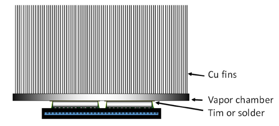
For multi-chip modules, a typical high heat flux thermal solution may look like the schematic diagram shown in
Figure 33 (adapted from [37]). Air-cooled heat sink modules are known to be highly reliable thermal management
solutions. However, the reliability is at the expense of a large areal and volumetric footprint due to the inferior
thermal properties of air, especially the thermal conductivity and low density. The air-cooled heat sink module system
comprises a sequential arrangement of thermal interface material (TIM), spreader and heat sink. The performance of
the heat sink is largely a function of heat spreading. To augment the cooling limit of an air-cooled heat sink, a high-
performing heat sink with vapor chamber and high-conducting TIM must be combined. The limit on the maximum
air flow is dictated by the acoustic constraints and the allowable pressure drop in the system. One example of
estimating air-cooling limits assumes a uniform heat flux at the devices; the maximum possible device heat flux is
estimated to be about 84 W/cm
2
[38] for a specific set of assumptions. However, more recent studies [39] have
utilized the limit on minimum inlet air temperature as dictated by the Telcordia GR63 standard and ASHRAE for
telecom applications (55°C) and data center applications (45°C) respectively, as well as including heat spreading
assumptions (vs uniform heat flux). Within these practical limitations, the efficient air-cooled module demands a
high-conductive TIM with a thin bond line and a highly efficient vapor chamber (with high dry-out heat flux) that
has a thin profile. A recent study [39] experimentally demonstrated a unit area junction to ambient air-cooled heat
sink limit of 0.8°C-cm
2
/W thermal resistance (this is a thermal resistance commensurate with 0.8°C temperature rise
across 1 cm
2
of area with 1W of heat dissipation). The heat sink housed a heat pipe in addition to the vapor chamber,
to efficiently move the heat to the lateral regions of the heat sink, thereby making fins more efficient and increasing
the efficiency of the overall heat sink. Higher heat flux levels may be possible through further optimization of the
March 2023 Thermal
HIR 2023 version (eps.ieee.org/hir) Chapter 20, Page 21 Heterogeneous Integration Roadmap
heat sink geometry and/or vapor chamber design and the TIM thermal resistance, or by relaxing the practical
constraints such as the allowable heat sink volume or air flow.
Figure 33: Figure adapted from [34] showing a schematic diagram of a heterogeneously integrated multi-chip module
with a Thermal Interface Material (TIM) or solder attachment and a vapor chamber.
In order to establish the air-cooling limit for differing physical form factor heat sink solutions, an in-house
experimental series was performed to arrive at a global equation. This equation describes the junction to incoming
air resistance impedance as a function of the flow parameters. The inlet air temperature was chosen based on the
Telcordia GR63 standard and ASHRAE for telecom application (55°C) and data center application (45°C)
respectively. Tests were also conducted for different thermal solutions that can be used in either 1U (1.75” industry
standard server) to 4U (7” tall industry standard server) data center server applications. The in-house test established
another level of confidence on the air-cooling limit in Figure 34 and Table 1, which is around 40-53 W/cm
2
for a
thermal budget of around 45°C- 50°C. Using the test result data points, the following equation was established [39]:
R*
JA
=192.8 (V
HS
/A
af
)
-1.258
F
-0.30
where:
R
JA
is Unit Area Junction to air resistance in °C cm
2
/W
F is flow speed in LFM (Linear Feet Per Minute)
V
HS
is heat sink volume
in cm
3
A
af
Air flow approaching area in cm
2
By employing the above equation, for both the 1U and 4U standard servers, respectively, the R
JA
was 1.22°C
cm
2
/W under a constrained thermal budget of 50°C from junction to inlet air (ambient). It was also noted that the
designer should account for the spreading resistance where it is varied based on the structure of the package and/or
the power map on the chip. Figure 34 shows reported data from [38] and the latest air and liquid cooling limits [39,
40]. Refai Ahmed et al. [39] developed the curves of thermal resistances based on a 1D resistance model. The
objective of the curves of thermal resistances in Figure 34 was to give an example of an engineering cost reduction
practice. This engineering practice is to present, at a target thermal resistance, a solution that has a high-performance
heat sink solution and low performance thermal interface materials, or vice versa. This was given as guidance for
the practitioner who needs to do cost optimization. However, to extend air cooling’s limit, the practitioner must use
both a high-performance heat sink and a low-resistance TIM similar to the work carried out in this study. Figure 34
was constructed based on the total available system resistance from junction to ambient. Resistance from junction to
inlet air (ambient) was varied from 0.5 to 0.05°C/W. From the known TIM and spreading resistance, the available
heat sink thermal resistance is determined and plotted.

March 2023 Thermal
HIR 2023 version (eps.ieee.org/hir) Chapter 20, Page 22 Heterogeneous Integration Roadmap
Figure 34: Heatsink thermal impedance, RS-A, versus chip heat flux
with regimes marked for different cooling technologies [28]
3.2.2 Liquid and two-phase cooling
There are several approaches to liquid cooling of electronic systems. These can be broadly classified into indirect
and direct liquid cooling. For direct (immersion) systems, the coolant comes into direct contact with the devices and
therefore the cooling material needs to be a dielectric. This could exclude water as the cooling medium and is
therefore a significant limitation in terms of achieving very high heat flux levels. To make water as a medium work
for such configurations would require electrically insulating technology (e.g. plated ground planes, sufficiently
thicker chips) to isolate the devices from the water. It is also a challenge to have the cooling fluid come into direct
contact with the electronic devices, since any organic materials in the system pose the risk of degradation and leaching
into the coolant over time. The advantage of direct liquid cooling is primarily the reduction of thermal resistances
such as those of heat spreaders and TIMs. Chip-scale cold plate designs with fluorocarbon cooling can be used with
heat flux levels of up to 100 to 300 W/cm
2
[41-44]. The range depends on specific design and system considerations.
Even higher heat flux levels may be achieved if cost and space limitations are expanded.
Indirect cooling is distinguished by the presence of a physical barrier between the devices and the coolant, thereby
eliminating concerns about chemical interactions between the coolant and the devices and also making the usage of
water (with additives) a possibility. Direct and indirect liquid cooling, both single-phase and two-phase, can be used,
with distinct advantages and disadvantages to each approach. Single-phase cooling systems are easier to design and
operate. However, when single-phase systems are used to cool multiple devices in series, the incoming coolant keeps
rising in temperature, which may be a limitation depending on the application. Two-phase systems, if well controlled,
have the advantage of operating at nearly uniform temperatures even when used serially to cool multiple modules.
Indirect water cooling can achieve significantly higher heat flux levels of up to 300 to 450 W/cm
2
for chip-scale water
jet impingement solutions.
A recent study [40] established a limit of 0.1°K cm
2
/W (based on chip area) for a separable remotely liquid cooled
module. The optimal values obtained for the fin thickness are within the range of 0.25-0.3 mm and the optimal
channel width was close to 0.4 mm. The study established a limit of Unit Area Thermal Resistance R
JA
= 0.35°C
cm
2
/W (based on chip area) corresponding to a chip heat flux of 170 W/cm
2
(marked in Figure 34) for a remote
cooled module for liquid cooling employing parallel channels operating below a constrained pressure drop value of
10kPa. From the series of detailed experiments, a correlation for Unit Area Thermal Resistance from junction to inlet
fluid ambient, R
JA
, was determined as follows:
R
JA
=0.47×FR
-0.276
where FR is the liquid flow rate in liters per minute, and the equation is valid between 0.3 < FR < 1.5
Table 1, including data adapted from [37] and more recent published data, provides a summary of cooling limits
for air, FC and water as well as the thermal resistance (air cooled module) and thermal insulation (water and FC).

March 2023 Thermal
HIR 2023 version (eps.ieee.org/hir) Chapter 20, Page 23 Heterogeneous Integration Roadmap
Table 1: Comparison of system cooling capabilities
Thermal solution High end chip scale heat
flux (based on chip area)
R
int
Chip to heat sink/cold
plate (based on chip area)
R
ext
heatsink/cold plate
(based on chip area)
Advanced multi-chip air
cooling with integrated
vapor chamber
0.85 W/mm
2
(uniform
heat flux)
Vapor chamber 0.267
°C/W (w/ Grease)
0.2 °C/W (w/ solder) for
Chip to fins
0.1 °C/W for Al
.069 °C/W for Cu
[34]
0.55 W/mm
2
(thermal
budget 50 ° C) [39]
chip area = 4 cm
2
Vapor chamber 0.03°C
cm
2
/W [45]
0.0375 °C cm
2
/W (TIM
20W/mK and 75 microns
thick) [31]
0.8 °C cm
2
/W for
Aluminum
[39]
Water cooled separable
module level cold plate
2.50 W/mm
2
(uniform
heat flux)
0.35 cm
2
K/W
Lid +TIM
0.128 cm
2
K/W
1.70 W/mm
2
(thermal
budget 50° C) Chip area =
4 cm
2
, heat sink base area
= 16 cm
2
[40]
0.2 °C cm
2
/W spreading
on 3mm thick Cu spreader
+ 0.0375 °C cm
2
/W (TIM
20W/mK and 75 microns
thick) [40]
0.1 °C cm
2
/W [40]
Water jet impingement
[46]
4.6 W/mm
2
N/A 0.025 cm
2
K/W
Water
immersion cooling [47]
5.62 W/mm
2
for a device
area of 12.5 mm
2
at
Thermal budget of 100 °C
Fluid temperature = 25 °C
(Power electronics)
N/A 0.18 °C cm
2
/W
Two phase (dielectric)
immersion cooling [47]
1 W/mm
2
for a device
area of 12.5 mm
2
at
Thermal budget of 50 °C
Fluid temperature = 25 °C
(Power electronics)
N/A 0.5 °C cm
2
/W
Micro channels in the
device with single phase
water flow [48]
About 7.90 W/,m
2
71 °C temp rise, Chip size
= 1 cm
2
N/A 0.09 °C cm
2
/W
Micro channels in the
device with two phase
[49]
About 10.20
W/mm
2
(uniform heat
flux)
58 °C temp rise
Chip size = 0.25cm
2
N/A 0.056 °C cm
2
/W
Water has a high thermal conductivity and specific heat capacity and therefore outperforms FCs. Compared to
the use of indirect liquid cooled cold plates that are attached (mounted) on a chip using a thermal interface material
(TIM), reduction in thermal resistance would require etching microchannels or fins in the silicon directly, as
demonstrated by Tuckerman and Pease [48] who demonstrated a heat flux of 790 W/cm
2
at a maximum temperature
rise of 71°C. Although this approach has not been commercialized, it may be considered to be close to the best
achievable ultimate heat flux level for silicon devices with longitudinal microchannels. Manifold-based
microchannel configurations discussed subsequently in this chapter outperform single-pass longitudinal arrays. This

March 2023 Thermal
HIR 2023 version (eps.ieee.org/hir) Chapter 20, Page 24 Heterogeneous Integration Roadmap
would be approximately true for 3D stacks with cooling liquid through the stack as well. For this case, the internal
thermal resistance is 0 and the external resistance will be a function of the microchannel design.
3.2.3 Summary of system cooling limits
Establishing the pragmatic limits on the most promising system cooling technologies in combination with the best
thermal interface materials becomes very important for understanding the thermal limits. A nominal summary
overview for the TIM and system (air and liquid) cooling technologies discussed in the previous two sections has
been combined to yield the analyses displayed in Figure 35.
Figure 35: Nominal summary overview for the TIM and system (air and liquid) cooling technologies
3.3 Embedded liquid cooling of chips and chip stacks
Embedded cooling [50] represents a third generation (“Gen3”) thermal management technology for electronic
circuits and was the focus of DARPA’s recent Near Junction Thermal Transport [51] and Intra/Interchip Enhanced
Cooling [52-53] thermal packaging programs. The DARPA Near-Junction Thermal Transport (NJTT) program,
initiated in 2011, was the first program to develop thermal management for the region within 100µm of the electrical
junction of a GaN transistor, to enable heat fluxes of greater than 10 kW/cm
2
while maintaining reliable junction
temperatures. Through technology developed in this program, specifically the transfer of GaN epitaxy to high thermal
conductivity diamond, the power handling capability of GaN HEMT devices was increased by greater than a factor
of 3 [54-59].
While the NJTT program made significant gains using high thermal conductivity substrates to spread the heat
close to the junction, it did not address the next link in the thermal resistance chain, i.e. extracting the heat from the
diamond and transferring that dissipated heat to an available coolant. The DARPA ICECool program [60], which
began in 2013 and is now nearing completion, combined embedded microfluidics with high thermal conductivity
substrates to reduce the thermal resistances in the entire package. The successful demonstration of embedded cooling
by three of the participating research teams is described in this section.
3.3.1 2D chip direct contact liquid cooling with hierarchical manifolds
Electronic devices have traditionally been cooled through the attachment of separate heat sinks. In this ‘remote
cooling’ architecture, the performance of the thermal management solution has become increasingly governed by
interfacial, conduction, and spreading thermal resistances incurred by the package and the mechanism of heat sink
attach. Trends in heterogeneous integration call for the development of transformative cooling strategies that embed
the thermal management solution directly within the device to alleviate hotspots. ‘Intrachip cooling’ strategies deploy
coolant channels directly in the electronic device, eliminating interfacial resistances but leaving little material
thickness available for heat spreading; this exposes the embedded microfluidic heat sink directly to the high heat
fluxes generated from the device. Dielectric working fluids are preferred for such systems because they minimize
the threat for electrical shorting.
As part of the DARPA ICECool Fundamentals program [60], researchers at Purdue University have demonstrated
dissipation heat fluxes exceeding 1000 W/cm² by feeding an array of high-aspect-ratio, intrachip microchannel heat
sinks in parallel with a dielectric coolant via a manifold for fluid distribution. The fabrication of suitably high aspect
ratio microchannels etched into the silicon test chip provides the necessary surface area enhancement to dissipate

March 2023 Thermal
HIR 2023 version (eps.ieee.org/hir) Chapter 20, Page 25 Heterogeneous Integration Roadmap
high heat fluxes at an allowable surface temperature rise; the microchannels are imbedded directly into the heated
substrate to reduce the parasitic thermal resistances due to contact and conduction resistances. Parallelization of the
flow across an array of short-flow-length microchannel heat sink elements serves to minimize the pressure drop across
the heat sink. This allows for flow boiling operation in the microscale channels, which would otherwise be prohibitive
due to pressure drop constraints.
A hierarchical manifold microchannel heat sink array test vehicle, with all flow distribution components
heterogeneously integrated, was fabricated to demonstrate thermal and hydraulic performance of this technology
(Figure 36, [61-62]). A silicon chip, with resistive heaters and local temperature sensors fabricated directly on the
opposite face, is cooled by a 3 × 3 array of microchannel heat sinks using dielectric HFE-7100. The heat sink
performance is characterized over a range of channel mass fluxes and channel geometries. At a mass flux of 2100
kg/m²s and for microchannel channel cross sections with widths of 33 μm and depths of 470 μm, uniform heat fluxes
up to 1020 W/cm² are dissipated over a 5 mm × 5 mm heated area, at chip temperatures less than 69°C above the
fluid inlet and at pressure drops less than 120 kPa. Experiments were also conducted for heat fluxes generated up to
2,700 W/cm² from a 200 μm × 200 μm hotspot heater overlaid on the background heat flux. This work demonstrates
the fabrication, integration, and characterization of hierarchical manifold microchannel heat sinks operating in the
two-phase regime.
3.3.2 Extreme heat flux micro-cooler for direct contact 2D
chip liquid cooling
Thermal-power challenges and increasingly expensive
energy demands pose threats to the historical rate of increase
in processor [66] and power electronics performance.
Energy-efficient computing [67] and heterogeneous
integration [68] promise substantial reduction in energy
demand for emerging and growing computing needs.
However, these conflicting trends have resulted in a
substantial increase in both heat flux >350 W/cm² and power
density, which reduced the efficacy of conventional cooling
technology solutions.
Figure 37 depicts the thermal resistance (cm²-K/W) versus
chip area for the state-of-the-art high heat flux (~1 kW/cm²)
cooling technologies, which indicates it is extremely
challenging to reject heat from large-area devices using
single/two-phase µ-channel coolers (2D and 3D manifold)
[63-73]. This originates for the presence of long traverse
paths for liquid delivery and vapor extraction as well as the
finite thickness of the liquid evaporation film (or thermal
boundary layer), which result in a large pressure drop and
increased junction temperature (or thermal resistance); note the trend shown by the yellow band, depicted in Figure
37.
A potential solution could be in the form of an Extreme Heat Flux µ-Cooler (EHFµ-C), depicted in Figures 38a
and 38b, that simply “scales up” a high heat-flux thin-wicking structure, either copper inverse opals (CIOs) [52] or
silicon pin fin arrays, to a large area EHFµ-C using 3D manifold liquid delivery and vapor extraction conduits [64-
75]. Two of the state-of-the-art technologies [63-64] have been developed at Stanford [63-66,72] since 2010 through
collaborations with Toyota, Ford, Google and IBM, and with funding from DARPA’s IceCool program and the NSF-
Figure 36: Hierarchical manifold microchannel heat sink
array: (a) three-dimension drawing of the test vehicle with a half-
symmetry section removed and fluid inlets (blue) and outlets (red)
shown; (b) zoomed-in view of the test vehicle with a quarter-
symmetry section removed showing the fluid flow paths in the test
chip; and (c) photograph of the test chip mounted to the PCB with
heaters and sensors face up. (d) Experimental characterization of
the base heat flux as a function of average chip temperature for a
heat sink with 33 μm ×470 μm cross section microchannels at
three different mass fluxes.

March 2023 Thermal
HIR 2023 version (eps.ieee.org/hir) Chapter 20, Page 26 Heterogeneous Integration Roadmap
Center for Power Optimization of Electro-Thermal Systems (POETS). Currently, Stanford is working on the next
generation of high performance EHFµ-Coolers (ARPA-e funded). The proposed EHFµ-C (Fig. 38) is produced by
bonding a 3D-manifold to a silicon substrate electro-plated with a copper inverse opal (CIO) wick. Liquid channels
deliver liquid to the CIO wick, where it is pulled in by capillary forces, and evaporates due to the high heat flux
~1kW/cm² at the substrate.
Figure 38a: The expected performance targets for EHFµ-Cooler, and that of the state-of-the-art devices including
Stanford’s previous work [63-64]. Critical heat flux levels are from 200 to 1000 W/cm². The EHFµ-Cooler represents more
than 10× reduction in thermal resistance, an unprecedented CHF >1 kW/cm² for water as working fluid, and can be scaled up
to large areas >10cm².
Figure 38: Schematic of the EHFµ-C concept: (a,b) front & sides cross section views. The EHFµ-Cooler is produced by
bonding a 3D-manifold to a silicon substrate electro-plated with a copper inverse opal (CIO) wick. Liquid channels deliver
liquid to the CIO wick, where it is pulled in by capillary forces, and evaporates due to the high heat flux ~1kW/cm² at the
substrate. (c) A schematic of Stanford’s “small-scale” test structure [52], (d) capable of removing 1600 W/cm², inset SEM
image of CIO with pore diameter ~ 5 µm.

March 2023 Thermal
HIR 2023 version (eps.ieee.org/hir) Chapter 20, Page 27 Heterogeneous Integration Roadmap
3.3.3 Embedded interlayer cooling for chip stacks with two-phase refrigerant
Embedded interlayer cooling technology provides a solution for cooling 3D chip stacks where a heat sink or cold
plate is inadequate for thermal management of 3D stacking of high-power chips because of their inability to cool
chips in the middle and bottom of the stack. This chip-embedded cooling technology circumvents that problem by
pumping a heat-extracting dielectric fluid into microscopic gaps, some no wider than a single strand of hair (~100
μm), between the chips at any level of the stack. The dielectric fluid used can come into contact with electrical
connections, so is not limited to one part of a chip or stack. This ability benefits chip stacks in terms of materials and
architecture, such as putting memory and accelerator chips on top of high-power chips in the stack as shown in Figure
39 which includes a fluid port to deliver fluid between the stacked dies.
Figure 39: High power 3D package with interlayer cooling [63]
The coolant is pumped into the chips, where it removes the heat from the chip by boiling from liquid-phase to
vapor-phase. It then re-condenses, dumping the heat to the ambient environment where the process begins again, as
shown in Figure 40. As this cooling system doesn’t need a compressor, it can operate at much lower power compared
to typical refrigeration systems.
Figure 40: Two Phase Pumped
Cooling System

March 2023 Thermal
HIR 2023 version (eps.ieee.org/hir) Chapter 20, Page 28 Heterogeneous Integration Roadmap
Two-phase flow boiling has long been proposed as a potential method for cooling high-performance computer
systems. A large body of work investigating and developing technologies appropriate for cooling electronics with
two phase flow boiling in parallel micro/mini-channels exists, but parallel channel two-phase flow is challenged by
instability issues, particularly with non-uniform power maps. This technique utilizes a significantly different
approach to embedded cooling. Rather than moving coolant from one edge of the die to the other through long
parallel channels, a dielectric coolant (R1234ze or similar) is fed in at the center of the die, moves through radially
expanding channels, and exits at the edges of the die. This approach provides better energy efficiency and maximum
critical heat flux with the resulting reduced flow path. The cooling capability was demonstrated on a specially
constructed thermal test vehicle (Figure 41 a,b,c,d) designed to mimic the heat generation capability of real
microprocessors without requiring actual transistor-based circuitry. In these studies, power densities of 350 W/cm²
within an area measuring 3.6 mm x 4.8 mm representing a microprocessor core and 200 μm x 200 μm hot-spot power
levels of more than 2 kW/cm² were shown to be effectively cooled with chip junction temperatures of < 60°C as
shown in Figure 42 [74-75].
Figure 41; Prototype for Embedded Refrigerant based
Interlayer cooling (a) Packaged thermal test Vehicle.
(b) Representative power map, (c) RTD numbers and
relative locations. (d) SEM image of the orifices and
radial expanding channels
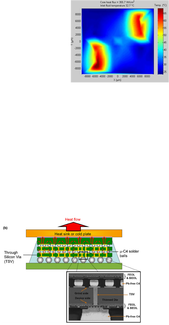
March 2023 Thermal
HIR 2023 version (eps.ieee.org/hir) Chapter 20, Page 29 Heterogeneous Integration Roadmap
Fig 42: Interpolated visualization of the temperature profile of the thermal test vehicle [75], with two diagonal quadrants
powered at 350 W/cm², Hot Spots 2000 W/cm² and Background 20 W/cm² heat flux. Total Power ~300 W.
3.4 Advanced thermal materials for thermal management
Several new materials are being explored from a research and development standpoint for enhancement of heat
spreading, thermal interfaces, and underfill materials as described in [76-78], for the various conduction layers of
heterogeneously integrated (and other) packages. Examples of such materials include cubic crystals, two-
dimensional layered materials, nanostructure networks and composites, molecular layers and surface
functionalization, and aligned polymer structures.
Figure 43 [76] depicts a 3D chip stack using advanced materials in the conduction heat flow path. The construction
includes details such as the front-end-of-line (FEOL) and back-end-of-line (BEOL) device and interconnect layers as
well as controlled collapse chip connections (C4) and smaller μ-C4 features. Of special note is typical epoxy-based
underfill materials that fill up the gaps between the 3D stacked dies. With low intrinsic thermal conductivities of
0.1–0.2 W/m-K [76] they yield a significant thermal resistance to the heat flow as also discussed previously in Section
2.2 (3D Chip Stack with Conduction Interfaces). Thus, new underfill materials or composites need to be developed
[76] with higher isotropic thermal conductivities to promote cross-plane heat conduction and die-to-die heat
dissipation, while also enhancing in-plane (2D) heat spreading to mitigate hot spots in the power sources.
While Figure 43 is a valid example of a high-performance package, this opportunity for new materials is very
much present for the Mobile space as well with inherent heat spreading challenges as discussed previously in Section
2.6 (Mobile Devices challenges). Indium Tin Oxide (ITO) is a material of choice for touch screens [76] in such
mobile devices, but more recently materials such as carbon nanotubes (CNTs), graphene, thinSi membranes, and
silver nanowires are being actively explored to solve thermal challenges [76].
Figure 43: 3D chip stack
with advanced materials in
conduction heat flow path [76]

March 2023 Thermal
HIR 2023 version (eps.ieee.org/hir) Chapter 20, Page 30 Heterogeneous Integration Roadmap
3.5 Thermomechanical modeling for heterogeneous integration (see also Chapter 15)
The power dissipation and power density in future 2D-3D packages is expected to increase and the cross-talk
between different components of the package will further aggravate the thermal management challenges. This will
necessitate development of a multi-physics simulation tool with closely coupled thermal, mechanical and electrical
models to enable iterative simulations and robust design. This tool should allow coupling between different scales,
e.g., die to package and package to system (board), to consider the effect of design at these different scales. High
heat flux components of packages will require single- or two-phase liquid cooling. The models for accurate prediction
of two-phase fluid flow have not been developed yet. Physics-based models in combination with machine learning
tools will be needed for high fidelity prediction of performance and design of these cooling technologies.
We discuss the needs and possible approaches for next-gen modeling and simulations tools. The vast majority of
thermal/thermomechanical design rules in electronics design and packaging are based on finite element simulations
post-electronic design. Robust thermomechanical models are not present in the electronic design and reliability flows,
thus necessitating significant margins from the designers. Here we suggest a paradigm shift to better model, optimize
and design for die and package level thermomechanical effects. The primary aim of this framework is to use a
repository of finite element simulations packaged through a neural network engine and abstracted into usable design
models. The following workflow (Figure 44) is proposed to enable this early integration of thermal and mechanical
models into design tools:
Definition of the design space and execution of FEM simulations with combinatorial and probabilistic input
parameters spanning geometrical descriptions, materials properties and interface/boundary conditions across
domains.
Training Data: Output FEM state distributions and fields (electric field, power density, temperature, stress,
strain etc.). Training and validation using an artificial neural network with feed-forward deep autoencoders
(DAE).
Deployment of the validated DAEs generated in (2) to accurately predict the non-linear and statistical
behavior of a design with minimum computational and setup overhead.
Figure 44: Thermal/Multiphysics Modeling for Heterogeneous Packages
Glass/Si based interposers or 3D packages with stacked die will allow integration of different functionalities with
a wide range of power dissipation in both space and time. The efficient thermal management of hot-spots will require
development of novel phase change materials, along with high-conductivity materials with anisotropic thermal
properties. In addition, next-generation packages will need novel dielectrics, insulators and conducting materials.
The accurate estimation of thermal properties of these materials and their interfaces will be necessary to develop
predictive models. First-principle simulations in combination with machine learning tools will be beneficial in
predicting properties of these materials with specification of uncertainty, which can be input to multi-physics
modeling tools to understand their effect on packages, e.g., Design Space Definition shown in the workflow above.
3.6 Advanced Liquid Cooling for next Generation data center integrated circuits
When it comes to cooling high density electronic devices including CPUs, GPUs, and FPGAs employed in a data
center (DC) server HW infrastructure, two phase (2P) immersion cooling using boiler plates (aka evaporators) and
direct contact liquid cooling using cold plates (aka water cooled microchannel heat sinks) outperform traditional air-
cooling techniques. Liquid cooling technologies using water or a 2-phase dielectric fluid with their innate high
volumetric heat capacities enable this superior heat transfer performance. A recently concluded study from Microsoft
[77] compares the thermal performance of a commercially available Intel multi core high density overclockable
desktop class CPU (i9-9900K) [78] against three different heat sinks employing three different cooling mediums. The
high core level heat flux (> 100 w/cm
2
) associated with this processor made this problem an attractive one especially
from a CPU core level thermal management standpoint. The influence of various operational and system parameters
on the CPU thermal performance including CPU core voltage, CPU core frequency, working fluid temperatures,
coolant flow rates and thermal interface materials (TIM) were evaluated. CPU benchmarking tests performed for
different DC workload scenarios offered a lot of insights into the CPU performance and its dependence on system
and operational constraints. At a cooling medium temperature of 34 ˚C for example, an over clocked air-cooled CPU
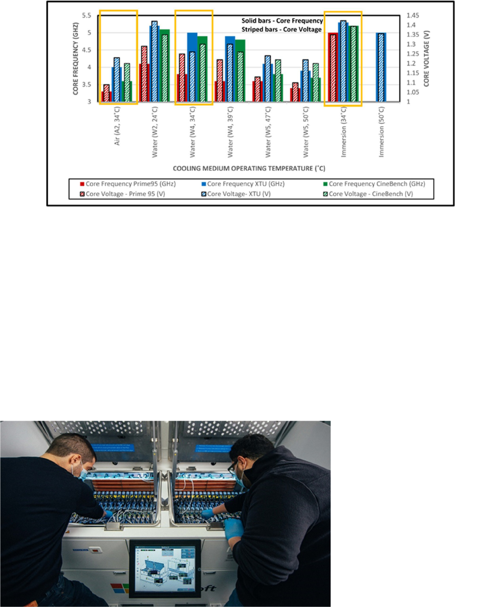
March 2023 Thermal
HIR 2023 version (eps.ieee.org/hir) Chapter 20, Page 31 Heterogeneous Integration Roadmap
(which is operating well past its TDP rating of 95W) throttled at a maximum clock frequency of 3300 MHz. The
water-cooled cold plates offered 41% higher clock rates compared to air cooled heat sink. 2-phase immersion cooling
yielded closer to 51% higher clock rates than their air-cooled counterpart at 34˚C. Using 2-phase immersion in certain
scenarios, the CPUs operated at stable frequencies well beyond 5200 MHz; a comparison can be found in the Figure
45.
Figure 45: CPU performance comparison among various cooling solutions and temperature conditions
Package level thermal resistance data suggested there is more room to gain further thermal budget through
advanced TIM and enhanced convective heat transfer surfaces. Also, it was observed that in the case of 2-phase
immersion cooling, the corresponding junction temperatures (Tj) are well below the maximum operating silicon
junction temperature (T
j, max
). This also indicates potentially lower leakage current from the silicon die/CPU which
can increase longevity and improve reliability of the HW device. This directly impacts the serviceability and
maintenance aspect of a scaled DC operation as well. In short, benefits from two phase immersion include better
efficiency, higher clock rates, lower fault rates, longer equipment life and so on.
In an immersion cooled DC, CPU overclocking increases the operating frequency of the cores. Rise in CPU core
frequency can be realized in a hyperscale DC environment in several ways including ‘computational bursting’ or
‘oversubscription of servers’ or ‘Virtual machine (VM) autoscaling’ [79]. Coupled with virtual core multiplexing,
this can “virtually” create extra cores from the same hardware, allowing us to aggressively oversubscribe CPUs.
Alternatively, this rise in frequency can be used to address load spikes in the workload’s CPU usage without requiring
auto-scaling. It is similarly possible to overclock GPU, memory, SSD, and other electronic components to improve
their performance. Furthermore, liquid immersion cooling brings new ways of server design and architecture and
brings opportunities for cross-layer optimizations across data center, server, and SW stack [80].
Figure 46: Operations at
immersion cooling tank

March 2023 Thermal
HIR 2023 version (eps.ieee.org/hir) Chapter 20, Page 32 Heterogeneous Integration Roadmap
In the case of liquid cooling utilizing copper microchannel cold plates, the CPU performance drops as shown in
the plot earlier, with increasing water inlet temperatures corresponding to different ASHRAE [81] water class
temperatures (W27, W32, W40 and W45). Water temperature in the lower ASHRAE class would require expensive
chiller operation to extract necessary peak CPU or HW performance, whereas the higher water class temperature
spectrum from ‘warm water-cooled data centers’ could operate better than air cooling and could also untap a potential
case for waste heat recovery from the DC exit water loop. Hence, at a DC level, liquid cooling is deemed as a
potential solution in not only enhancing the DC/device densification but also improving the energy efficiency and
performance of the DC, and also weighed in as a serious contendor to reliable and noiseless DC operation.
Finally, as we get into the era of multi-chip modules (MCMs), chiplets [82], and heterogeneously integrated (HI)
and 3D stacked devices, advanced liquid cooled DC infrastructure is certainly regarded as an enabler of future
generation devices and business markets. Microsoft’s Research and Advanced Development Team (RAD) has been
engaging with industry and academia to advance the state-of-the-art technology enablers for scaling the next
generation of heterogeneously integrated systems, including for both 2.5D and 3D systems, by looking to develop
advanced thermal management solutions such as microfluidics cooling technology and pushing the boundaries of
advanced interconnect technology containing through silicon vias (TSVs) and its associated density. Regarding 2.5D
systems technology enablement documented in this article [83], fabrication recipes were developed, demonstrating
monolithic 2.5D microfluidic cooling, where silicon micro pin-fins are etched directly into the backside of a
monolithic CMOS - Intel Core i7- 8700K CPU containing 6 cores with a maximum core heat flux of roughly about
250 W/cm
2
. The overclocked CPU dissipated up to 215W of power, much higher than its rated TDP of 95W while
being cooled by room temperature de-ionized (DI) water. Up to 44.4% reduction in junction-to-inlet thermal
resistance was demonstrated, while using only 0.3× of volumetric coolant flow per Watt of power dissipated in the
CPU compared to a conventional cold-plate.
Figure 47: Microfluidic Cooling Solutions
Furthermore, for 2.5D Monolithic systems, higher sustained core frequencies were demonstrated, even when being
cooled with elevated inlet temperatures, showing the potential for more efficient datacenter operations without the
need for expensive and energy intensive refrigeration loops (Figure 47). These results point towards a more scalable,
efficient cooling solution, which can unlock higher power, more efficient compute systems and architecture types,
while minimizing the environmental impacts by reducing thermal management overheads . These attributes support
the Microsoft sustainability pledges of reducing their historic carbon emissions associated with its operation by 2050
(and that includes scope 1, scope 2 and scope 3 emissions) [84]
and replenish their facilities with more water than
what been used for its services by 2030 [85].
3.7 Innovative manufacturing method for silicon microchannel cooling technology
Photolithographic techniques are an indispensable tool in the modern world for creating micro-nanoscale chips
for electronics. Lithography is also used to create structures for applications in optics, photonics, microfluidics,
biology, chemistry, battery technology, sorption-desorption, water harvesting, desalination, and catalysis. However,
conventional photolithographic methods suffer from a major limitation – they are unable to create multi-level or
multi-depth, hierarchical, 3D structures in the substrate of more than a few microns in height. Usually, the lithography
process flow employs the following steps – (1) Coating – This involves dispensing a photosensitive polymer (called
photoresist or PR) on the substrate spinning at high RPM, which leads to a very thin (4 – 10um) conformal coat of
the PR on the substrate; (2) Exposure and Development – UV light is then used to expose a 2D pattern on the PR.
The UV light selectively changes the polymerization in the PR. The next stage (called development) involves washing

March 2023 Thermal
HIR 2023 version (eps.ieee.org/hir) Chapter 20, Page 33 Heterogeneous Integration Roadmap
away the exposed part of the PR using the developer solution. After the exposure and development phase, we are
left with a pattern of PR on the substrate.
This pattern can now be imprinted/etched into the substrate by etching the substrate and using the PR left behind
as a mask. To create multiple levels in the substrate, a LELE (Litho-Etch-Litho-Etch) process flow is used where the
lithography and etching step must be repeated multiple times, with a different exposing design and etching duration
in every step. The major hurdle arises in the second round of lithography, where PR spin coating is attempted on a
substrate with features already etched into it. The spinning process on an already etched wafer is satisfactory (thin
and uniform) when the PR thickness (4 – 10μm) is much larger compared to the etch height of the features. Thus, in
some cases of IC fabrication, where the already etched feature height is ≤ 1 – 4μm, the LELE process works perfectly.
However, in several useful applications of microfluidics, liquid cooling, optics and semiconductor fabrication, these
etch depths are of the micro-meso scale and can range anywhere from 10μm to 500 – 600μm. PR spinning on larger
step heights (more than 5 – 10μm) lead to unsatisfactory coating. Several problems like streaking, fingering, and
incomplete coverage mar the spin coating process in the second rounds of lithography. This causes failure of the
downstream exposure process, whose success relies exclusively on the uniformity of the PR coat – thus leading to
failure of the overall process.
Figure 48: Manufacturing process for making silicon microchannels
In this context, it was recognized that the failure occurs primarily because the PR thickness (4 – 10um) is often
much smaller than the features etched in the substrate. A solution was envisioned wherein the 3D multi-level pattern
would first be created by LELE processing not directly on the substrate but rather a much thinner sacrificial layer on
the substrate. SiO
2
was found to be one of the best candidate materials for this sacrificial layer since Si:SiO
2
etch
selectivity during reactive ion etching is 200 – 300, which indicates that using 3um of SiO
2
layer, multi-level
structures can be etched in the silicon substrate underneath of height > 500um. A novel process flow was reported
where an ultra-thin sacrificial layer of SiO
2
was first deposited/grown in between the PR and the silicon wafer; the
SiO
2
layer now acting as the masking material during the deep Si etching process instead of PR. Multiple rounds of
conventional LELE lithography are used to pattern this newly introduced SiO
2
mask layer; this time PR thickness is
larger than the step height in the SiO
2
underneath, and the conformal spin coating process is carried out without any
difficulties. After this, by deep Si etching, this 3D multi-level pattern in the SiO
2
gets scaled vertically by the etch
selectivity (200 – 300) and transferred to the silicon.
The novel process flow reported uses very commonly employed cleanroom-based tools like lithography, SiO
2
and
Si etching. It is easily characterizable, requiring us to only characterize the SiO
2
and Si etch step. This process also
eliminates many of the uncontrollable parameters associated with grayscale lithography which makes knowledge
transfer from one lab to another easy. The process flow also makes 3D structures via one-shot deep Si etching based
pattern transfer, thus reducing failure due to handling fragile wafers; this increases yield to 90%. The process flow
was verified to be highly repeatable and reliable; additionally, SiO
2
etch characterization data is also provided as a

March 2023 Thermal
HIR 2023 version (eps.ieee.org/hir) Chapter 20, Page 34 Heterogeneous Integration Roadmap
starting point for other users. This method can be extended to other pairs of compatible substrates (glass, sapphire,
PDMS, polymers) and sacrificial hard-masks (Al, Si
x
N
y
, Al
2
O
3
etc).
4.0 Thermal Technical Working Group Contributors
Madhusudan Iyenga
r
Andy Mackie Avi Ba
r
-Cohen Ali Merrikh
Amr S. Helmy Azmat Malik Bahgat G. Sammakia Baratunde Cola
Baris Dogruoz Benson Chan Bharath Ramakrishnan Bob Corne
r
Bill Bottoms Callum Middleton Carl Zweben Cheng Chen
Chris Malone Cleverson Souza Chave Craig Green Damena Agonafe
r
Dereje Agonafe
r
Devdatta Kulkarni Dhruv Singh Don Drape
r
Eduardo De Los Heros Eric Dede Erik Yen Gamal Refai-Ahmed
Herman Oprins Husam Alissa Jamal Yagoobi Jason Strade
r
Jaechoon Kim Justin A. Weibel Kamal Sikka Kanad Ghose
Kenneth Goodson Kevin P. Drummond Kuo-Huey Chen Leila Choobineh
Li Shi Luu Nguyen Man Prakash Gupta Mark Hempstead
Mehdi Asheghi Michael Barako Michael J. Ellsworth Norman Chang
Peter de Bock Ravi Mahajan Raymond Fillion Rockwell Hsu
Satish Kuma
r
Sreekant.Narumanchi Sivasanka
r
Sougata Hazra
Srikanth Rangarajan Suresh V. Garimella Taehwan Kim Tahir Cade
r
Timothy Chaine
r
Vadim Gektin Venkatesh Avula Victor Chiriac
Weihua Tang Wei Wang William Chen Yin Hang
Yoonjin Won Yogi Joshi Yunhyeok I
m
5.0 References
[1] Communications with R. Mahajan and W. Tang, Intel Corporation, 2020.
[2] Swaminathan R. & Mahajan R., HIR_ECTC, 2018).
[3] Sangbeom Cho, Venky Sundaram, Rao Tummala, Yogendra Joshi, (2016) "Multi-scale thermal modeling of glass
interposer for mobile electronics application", International Journal of Numerical Methods for Heat & Fluid Flow, Vol. 26
Issue: 3/4, pp.1157-1171).
[4] Kyomin Sohn, Won-Joo Yun, Reum Oh, Chi-Sung Oh, Seong-Young Seo, Min-Sang Park, Dong-Hak Shin, Won-Chang
Jung, Sang-Hoon Shin, Je-Min Ryu, Hye-Seung Yu, Jae-Hun Jung, Hyunui Lee, Seok-Yong Kang, Young-Soo Sohn,
Jung-Hwan Choi, Yong-Cheol Bae, Seong-Jin Jang, and Gyoyoung Jin, 2017, A 1.2 V 20 nm 307 GB/s HBM DRAM
With At-Speed Wafer-Level IO Test Scheme and Adaptive Refresh Considering Temperature Distribution, IEEE Journal
of Solid State Circuits, Vol. 52, No. 1, January.
[5] W. Bogaerts and L. Chrostowski, 2018, "Laser Photonics and Reviews", DOI: 10.1002/lpor.201700237.
[6] Stephane Bernabe-LETI-CEA, ECTC, 2014.
[7] USDRIVE Electrical and Electronics Technical Team Roadmap, 2017,
https://energy.gov/sites/prod/files/2017/11/f39/EETT%20Roadmap%2010-27-17.pdf.
[8] H. P. J. De Bock, J. T. Labhart, S. S. Chauhan, G. C. Kirk, and J. H. Kim, “Thermal interface devices,” US9615486B2,
2017.
[9] Power Electronics Thermal Management Chapter I.16, Electrification FY17 Annual
Report,https://www.energy.gov/sites/prod/files/2018/05/f52/Electrification_FY2017_APR_Final.compressed.pdf.
[10] Gu, Xiaoxiong, et al. "Antenna-in-package design and module integration for millimeter-wave communication and 5G."
VLSI Design, Automation and Test (VLSI-DAT), 2018 International Symposium on. IEEE, 2018.
[11] Green, Craig E., Leonardo Prinzi, and Baratunde A. Cola. "Design and evaluation of polymer-carbon nanotube composites
for reliable, low resistance, static and dynamic thermal interface materials." Thermal and Thermomechanical Phenomena
in Electronic Systems (ITherm), 2016 15th IEEE Intersociety Conference on. IEEE, 2016.
[12] Cameron Nelson, Jesse Galloway, 2018, Package Thermal Challenges Due to Changing Mobile System Form Factors,
IEEE Semi Therm Conference.
[13] “Ultra High Density SoIC with Sub-micron Bond Pitch,” Y. Chen, C. Yang, C. Kuo, M. Chen, C. Tung, W. Chiou, D. Yu,
TSMC, ECTC, 2020.
[14] “Advanced Packaging Technologies for Heterogeneous Integration (HI)”, R. Mahajan, S. Sane, Intel, Hot Chips, 2021.
[15] “A Thermal Machine Learning Solver for Chip Simulation”, R. Ranade, H. He, J. Pathak, N. Chang, A. Kumar, J. Wen,
IEEE MLCAD,2022.

March 2023 Thermal
HIR 2023 version (eps.ieee.org/hir) Chapter 20, Page 35 Heterogeneous Integration Roadmap
[16] “DNN-based Fast Static On-chip Thermal Solver”, J. Wen, S. Pan, N. Chang, W. Chuang, W. Xia, D. Zhu, A. Kumar, E.
Yang, K. Srinivasan, Y. Li, IEEE SEMI-THERM, 2020.
[17] “ML-based Fast On-chip Transient Thermal Simulation for Heterogeneous 2.5D/3D IC Designs”, N. Chang, A. Kumar, J.
Wen, H. He, S.Pan, D. Geb, W. Xia, S. Asgari, M. Abarham, Q. Li, Y. Li, Z. Feng, IEEE VLSI-DAT, 2022
[18] “On-chip Transient Hot Spot Detection with a Multiscale ROM in 3DIC Designs”, D. Geb, S. Asgari, A. Kumar, J. Wen,
N. Chang, S. Pan, M. Abarham, H. He, V. Gandhi, IEEE ECTC, 2022
[19] A. Hankin, D. Werner, M. Amiraski, J. Sebot, K. Vaidyanathan and M. Hempstead, "HotGauge: A Methodology for
Characterizing Advanced Hotspots in Modern and Next Generation Processors," 2021 IEEE International Symposium on
Workload Characterization (IISWC), 2021, pp. 163-175, doi: 10.1109/IISWC53511.2021.00025
[20] S. Li, J. H. Ahn, R. D. Strong, J. B. Brockman, D. M. Tullsen and N. P. Jouppi, "McPAT: An integrated power, area, and
timing modeling framework for multicore and manycore architectures," 2009 42nd Annual IEEE/ACM International
Symposium on Microarchitecture (MICRO), 2009, pp. 469-480.
[21] R. Zhang, M. R. Stan, and K. Skadron, "HotSpot 6.0: Validation, Acceleration and Extension." University of Virginia,
Tech. Report CS-2015-04
[22] F. Terraneo, A. Leva, W. Fornaciari, M. Zapater and D. Atienza, "3D-ICE 3.0: Efficient Nonlinear MPSoC Thermal
Simulation With Pluggable Heat Sink Models," in IEEE Transactions on Computer-Aided Design of Integrated Circuits
and Systems, vol. 41, no. 4, pp. 1062-1075, April 2022, doi: 10.1109/TCAD.2021.3074613
[23] T. Kim et al., "Thermal Modeling and Analysis of High Bandwidth Memory in 2.5D Si-interposer Systems," 2022 21st
IEEE Intersociety Conference on Thermal and Thermomechanical Phenomena in Electronic Systems (iTherm), San Diego,
CA, USA, 2022, pp. 1-5, doi: 10.1109/iTherm54085.2022.9899586.
[24] Prasher, R. Proc IEEE, 2006, 94, 8, 1571–1586.
[25] Bar-Cohen, A., et al. J. Electron. Packaging. 2015, 137, 040804-1.
[26] Goodson, K.E. Science, 2007, 315, 5810, 342–343.
[27] Barako, M.T., et al. ACS Appl. Mater. Interfaces, 2017, 9, 42067-42074.
[28] Le, M.T. and Huang, S.C., 2015. Thermal and mechanical behavior of hybrid polymer nanocomposite reinforced with
graphene nanoplatelets. Materials, 8(8), pp.5526-5536] [REF: https://www.azonano.com/article.aspx?ArticleID=3206].
[29] Won, Y., et al. Proc. Natl. Acad. Sci. U.S.A. 2013, 110, 20426–20430.
[30] Won, Y., et al. Carbon. 2012, 50(2), 347-355.
[31] G. Refai-Ahmed, H. Do, B. Philofsky, and J. Strader, 2018, Extending the performance of high heat flux 2.5D and 3D
packaging from component-system interaction, 19th International Conference on Thermal, Mechanical and Multi-Physics
Simulation and Experiments in Microelectronics and Microsystems (EuroSimE), Apr. pp. 1–6, doi:
10.1109/EuroSimE.2018.8369893.
[32] Lee, J., Won, Y., et al. 2018, submitted.
[33] Idumah, C. I., Hassan, A. Rev. Chem. Eng. 2016, 32, 413−457.
[34] Pham, Q., Won, Y., et al. Scientific Reports. 2017, 7, 10465.
[35] Hawkeye, M. M., et al. John Wiley & Sons, Ltd.: Chichester, UK, 2014.
[36] Evan Fleming, Iskandar Kholmanov, Li Shi, 2018, Enhanced specific surface area and thermal conductivity in ultrathin
graphite foams grown by chemical vapor deposition on sintered nickel powder templates, Carbon 136 (2018) 380-386.
[37] Ellsworth Jr, Michael J., and R. E. Simons. "High powered chip cooling—Air and beyond." Electron. Cooling 11, no. 3
(2005): 14-22.
[38] Saini, M., and Webb, R.L., “Heat Rejection Limits of Air-Cooled Plane Fin Heat Sinks for Computer Cooling,” IEEE
Trans. Components and Packaging Technologies, Vol. 26, No. 1, 2003.
[39] G. Refai-Ahmed, H. Do, Y.Hadad, S. Rangarajan, B. Sammakia, T. Cader, 2020, Establishing Thermal Air-Cooled Limit
for High Performance Electronic Devices, 22nd IEEE Electronics Packaging Technology Conference (EPTC).
[40] G. Refai-Ahmed, H. Do, Y.Hadad, S. Rangarajan, B. Sammakia, T. Cader, 2020, Establishing the Single-Phase Cooling
Limit for Liquid-Cooled High Performance Electronic Devices, IEEE 21st Electronics Packaging Technology Conference
(EPTC).
[41] Simons, R.E., “Estimating Parallel Plate-Fin Heat Sink Thermal Resistance,” ElectronicsCooling, Vol. 9, No. 1, 2003.
[42] Simons, R.E., “Estimating Parallel Plate-Fin Heat Sink Pressure Drop,” ElectronicsCooling, Vol. 9, No. 2, 2003.
[43] Copeland, D., “Review of Low Profile Cold Plate Technology,” Electronics Cooling Magazine, Vol. 11, No. 2, May,
2005, pp. 14-18.
[44] Colgan, E.G., Furman, M., Gaynes, M., Graham, W., LaBianca, N., Magerlein, J.H., Polastre, R.J., Rothwell, M.B.,
Bezama, R.J., Chaudhary, R., Marston, K., Toy, H., Wakil, J., Zitz, J., and Schmidt, R., “A Practical Implementation of
Silicon Microchannel Coolers for High Powered Chips,” Proceedings of the 21st Annual IEEE Semiconductor Thermal
Measurement and Management Symposium, San Jose, CA, USA, March 15-17, 2005, pp. 1-7.
[45] G. Meyer, 2017, Heat Pipes and Vapor Chambers - Design Guidelines, Presentation at the Semitherm Conference
https://semi-therm.org/wp-content/uploads/2017/04/Heat-Pipe-Vapor-Chamber-Heat-Sink-Design-Guidelines-Thermal-Live-
2016.pptx.pdf.”
[46] Campbell, L.A., Ellsworth Jr., M.J., Iyengar, M., Simons, R.E., and Chu, R.C., “Experimental Investigation of the Heat
Transfer Performance of Arrays of Round Jets with Sharp-Edged Orifices and Peripheral Effluent; Convective Behavior of

March 2023 Thermal
HIR 2023 version (eps.ieee.org/hir) Chapter 20, Page 36 Heterogeneous Integration Roadmap
Water on a Heated Silicon Surface,” Proceedings of the 2005 ASME Summer Heat Transfer Conference, San Francisco,
CA, USA, July 17-22, 2005
[47] P. Birbarah et al., 2020, Water immersion cooling of high power density electronics,Int. J. Heat Mass Transf., vol. 147, p.
118918, Feb. 2020, doi: 10.1016/j.ijheatmasstransfer.2019.118918.
[48] D. B. Tuckerman and R. F. W. Pease, 1981, High-performance heat sinking for VLSI,” IEEE Electron Device Lett., vol. 2,
no. 5, pp. 126–129, May 1981, doi: 10.1109/EDL.1981.25367.
[49] K. P. Drummond et al., 2018, Characterization of hierarchical manifold microchannel heat sink arrays under simultaneous
background and hotspot heating conditions, Int. J. Heat Mass Transf., vol. 126, pp. 1289–1301, Nov. 2018, doi:
10.1016/j.ijheatmasstransfer.2018.05.127.
[50] A. Bar-Cohen, J. J. Maurer, D. H. Altman, 2017, “Gen3 Embedded Cooling for High Power RF Components”, Keynote
Paper, Proceedings IEEE COMCAS, Tel Aviv, Israel.
[51] Near Junction Thermal Transport (NJTT), DARPA-BAA-11-09, posted Nov. 2010.
[52] Intrachip/Interchip Enhanced Cooling Fundamentals (ICECool Fundamentals), DARPA-BAA-12-50, posted June 2012.
[53] Intrachip/Interchip Enhanced Cooling Applications (ICECool Applications), DARPA-BAA-13-21, posted February 2013.
[54] M. Tyhach, D. Altman, S. Bernstein, R. Korenstein, J.-W. Cho, K. E. Goodson, D. Francis, F. Faili, F. Ejeckam, S.Kim, S.
Graham, "S2-T3: Next generation gallium nitride HEMTs enabled by diamond substrates." In IEEE Lester Eastman
Conference on High Performance Devices (LEC) pp. 1-4 (2014).
[55] J. Pomeroy, M. Bernardoni, A. Sarua, A. Manoi, D.C. Dumka, D.M. Fanning, M. Kuball, "Achieving the best thermal
performance for GaN-on-Diamond," in CSICS (2013).
[56] E. Bozorg-Grayeli, A. Sood, M. Asheghi, V. Gambin, R. Sandhu, T. I. Feygelson, B. B. Pate, K. Hobart, and K. E.
Goodson. "Thermal conduction inhomogeneity of nanocrystalline diamond films by dual-side thermoreflectance." Applied
Physics Letters, Vol. 102, no. 11, pp. 111907 (2013).
[57] J.E. Graebner, S. Jin, G.W. Kammlott, J.A. Herb, C.F. Gardinier. "Large Anisotropic Thermal Conductivity in Synthetic
Diamond Films." Nature, Vol. 359 pp. 401-403, (1992).
[58] A. Bar-Cohen, J.J. Maurer, and A. Sivananthan, Near-Junction Microfluidic Thermal Management of RF Power
Amplifiers, IEEE International Conference on Microwaves, Communications, Antennas, and Electronic Systems
(COMCAS 2015) (Tel Aviv, Israel, 2015).
[59] M. Tyhach, D. Altman, S. Bernstein, "GaN on Diamond Technology: Impact and Challenges of Next Generation GaN,"
presented in ASME InterPACK (2015).
[60] A. Bar-Cohen, J.J. Maurer, J.G. Felbinger, DARPA’s intra/interchip enhanced cooling (ICECool) program, Proceedings of
the Compound Semiconductor Manufacturing Technology Conference (CS MANTECH), (2013) 171-174.
[61] K. P. Drummond, D. Back, M. D. Sinanis, D. B. Janes, D. Peroulis, J. A. Weibel, and S. V. Garimella, A hierarchical
manifold microchannel heat sink array for high-heat-flux two-phase cooling of electronics, International Journal of Heat
and Mass Transfer 117, pp. 319–330, 2018.
[62] K. P. Drummond, D. Back, M. D. Sinanis, D. B. Janes, and D. Peroulis, J. A. Weibel, and S. V. Garimella,
Characterization of hierarchical manifold microchannel heat sink arrays under simultaneous background and hotspot
heating conditions, International Journal of Heat and Mass Transfer 126A, pp. 1289-1301, 2018.
[63] Palko, J.W., Zhang, C., Wilbur, J.D., Dusseault, T.J., Asheghi, M., Goodson, K.E. and Santiago, J.G., 2015, “Approaching
the limits of two-phase boiling heat transfer: High heat flux and low superheat,” Applied Physics Letters, 107(25),
pp.253903.
[64] Jung, K.W., Kharangate, C.R., Lee, H., Palko, J., Zhou, F., Asheghi, M., Dede, E.M., Goodson, K.E., 2019,” Embedded
Cooling with 3D Manifold for Vehicle Power Electronics,” Int. J. Heat Mass Transf. 130, pp. 1108-19.
[65] Ćoso, D., Srinivasan, V., Lu, M.C., Chang, J.Y. and Majumdar, A., 2012. Enhanced heat transfer in biporous wicks in the
thin liquid film evaporation and boiling regimes. Journal of Heat Transfer, 134(10), pp.101501.
[66] Hwang, G.S., Fleming, E., Carne, B., Sharratt, S., Nam, Y., Dussinger, P., Ju, Y.S. and Kaviany, M., 2011. Multi-artery
heat-pipe spreader: Lateral liquid supply,” Int. J. Heat Mass Transf., 54(11-12), pp.233440.
[67] Nam, Y., Sharratt, S., Cha, G. and Ju, Y.S., 2011. Characterization and modeling of the heat transfer performance of
nanostructured Cu micropost wicks. Journal of Heat Transfer, 133(10), pp.101502.
[68] Cai, Q. and Chen, Y.C., 2012, “Investigations of biporous wick structure dryout,” Journal of Heat Transfer, 134(2),
pp.021503.
[69] Semenic, T. and Catton, I., 2009, “Experimental study of biporous wicks for high heat flux applications,” Int. J. Heat Mass
Transf. 52, pp.5113-5121.
[70] Weibel, J.A., Garimella, S.V. and North, M.T., 2010, “Characterization of evaporation and boiling from sintered powder
wicks fed by capillary action,” Int. J. Heat Mass Transf., 53(19-20), pp.4204-4215.
[71] Bae, D.G., Mandel, R.K., Dessiatoun, S.V., Rajgopal, S., Roberts, S.P., Mehregany, M. and Ohadi, M.M., 2017,
”Embedded two-phase cooling of high heat flux electronics on silicon carbide (SiC) using thin-film evaporation and an
enhanced delivery system (FEEDS) manifold-microchannel cooler,” In Thermal and Thermomechanical Phenomena in
Electronic Systems (ITherm), 2017 16th IEEE Intersociety Conference on (pp. 466-472).
[72] Jung, K.W., Jih, E., Iyengar, M., Asheghi, M., Malone, C., Man Prakash, G., Goodson, K.E., 2018, “CFD modeling of
embedded cooling with 3D manifold for vehicle power electronics”, Ongoing work at Stanford.

March 2023 Thermal
HIR 2023 version (eps.ieee.org/hir) Chapter 20, Page 37 Heterogeneous Integration Roadmap
[73] Drummond, K.P., Back, D., Sinanis, M.D., Janes, D.B., Peroulis, D., Weibel, J.A., Garimella, S.V., 2018,
“Characterization of hierarchical manifold microchannel heat sink arrays under simultaneous background and hotspot
heating conditions,” Int. J. Heat Mass Transf. 126, pp. 1289–1301.
[74] Timothy J. Chainer, Mark D. Schultz, Pritish R. Parida, and Michael A. Gaynes, 2017, Improving Data Center Energy
Efficiency With Advanced Thermal Management, IEEE Transactions on Components, Packaging, and Manufacturing
Technology, Vol. 7, No. 8, August 2017.
[75] Schultz, M., Yang, F., Colgan, E., Polastre, R., Dang, B., Tsang, C., Gaynes, M., Parida, P. R., Knickerbocker, J. and
Chainer, T., “Embedded Two-Phase Cooling of Large 3D Compatible Chips with Radial Channels”, Journal of Electronic
Packaging, vol. 138(2), 2016.
[76] Arden L. Moore, and Li Shi, 2014, Emerging challenges and materials for thermal management of electronics, Materials
Today Volume 17,Number 4 May.
[77] CPU Overclocking: A Performance Assessment of Air, Cold Plates, and Two-Phase Immersion Cooling | IEEE Journals &
Magazine | IEEE Xplore B. Ramakrishnan et al., "CPU Overclocking: A Performance Assessment of Air, Cold Plates, and
Two-Phase Immersion Cooling," in IEEE Transactions on Components, Packaging and Manufacturing Technology, vol.
11, no. 10, pp. 1703-1715, Oct. 2021, doi: 10.1109/TCPMT.2021.3106026.
[78] Intel Core i99900K Processor 16M Cache up to 5.00 GHz Product Specifications
[79] Cost-Efficient Overclocking in Immersion-Cooled Datacenters | IEEE Conference Publication | IEEE Xplore M. Jalili et
al., "Cost-Efficient Overclocking in Immersion-Cooled Datacenters," 2021 ACM/IEEE 48th Annual International
Symposium on Computer Architecture (ISCA), 2021, pp. 623-636, doi: 10.1109/ISCA52012.2021.00055.
[80] To cool datacenter servers, Microsoft turns to boiling liquid
[81] ASHRAE: TC9.9 Emergence and Expansion of Liquid Cooling in Mainstream Data Centers (ashrae.org)
[82] AMD EPYC 7003 Processors (Data Sheet)
[83] Integrated Silicon Microfluidic Cooling of a High-Power Overclocked CPU for Efficient Thermal Management | IEEE
Journals & Magazine | IEEE Xplore S. Kochupurackal Rajan, B. Ramakrishnan, H. Alissa, W. Kim, C. Belady and M. S.
Bakir, "Integrated Silicon Microfluidic Cooling of a High-Power Overclocked CPU for Efficient Thermal Management,"
in IEEE Access, vol. 10, pp. 59259-59269, 2022, doi: 10.1109/ACCESS.2022.3179387.
[84] Microsoft will be carbon negative by 2030 - The Official Microsoft Blog
[85] Microsoft will replenish more water than it consumes by 2030 - The Official Microsoft Blog
Edited by Paul Wesling
